You are currently viewing SemiWiki as a guest which gives you limited access to the site. To view blog comments and experience other SemiWiki features you must be a registered member. Registration is fast, simple, and absolutely free so please,
join our community today!
            WP_Term Object
(
    [term_id] => 24
    [name] => TSMC
    [slug] => tsmc
    [term_group] => 0
    [term_taxonomy_id] => 24
    [taxonomy] => category
    [description] =>
    [parent] => 158
    [count] => 634
    [filter] => raw
    [cat_ID] => 24
    [category_count] => 634
    [category_description] =>
    [cat_name] => TSMC
    [category_nicename] => tsmc
    [category_parent] => 158
    [is_post] =>
)

WP_Term Object
(
    [term_id] => 24
    [name] => TSMC
    [slug] => tsmc
    [term_group] => 0
    [term_taxonomy_id] => 24
    [taxonomy] => category
    [description] =>
    [parent] => 158
    [count] => 634
    [filter] => raw
    [cat_ID] => 24
    [category_count] => 634
    [category_description] =>
    [cat_name] => TSMC
    [category_nicename] => tsmc
    [category_parent] => 158
    [is_post] =>
)
What does mango beer have to do with semiconductor design and manufacturing? At a table of beer drinkers from around the world I would have never thought fruity beer would pass a taste test, not even close. As it turns out, the mango beer is very good! Same goes for 20nm planar devices. “Will not work”, “Will not yield”, “Will not scale”,… Read More
Behind great humor often lies irony. In the midst of a struggle by the European Union to extract $1.3B from Intel in an ages old Anti-Trust case, the latter makes a strategic move to embolden the Dutch firm ASML to accelerate the development of 450mm and EUV and thus save a continental jewel. What now say EU? When disfunction and bankruptcy… Read More
Thanks to SemiWiki readers for the feedback and comments on the previous “Introduction to FinFET Technology” posts – very much appreciated! The next installment on FinFET modeling will be uploaded soon.
In the interim, Dan forwarded the following link to me “ Intel’s FinFETs too complicated and difficult, says … Read More
My luck continues as I missed last week’s typhoon. Fortunately it did not disrupt the annual Dragon Boat Festival. More than just a Chinese tradition, dragon boat racing is an international sports event with teams from around the world coming to Taiwan every year. It is very exciting with the colorful dragon boats and the wild beating… Read More
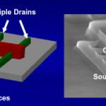
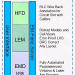
Lorentz Solution presented at TSMC’s DAC 2012 Open Innovation Platform Theater. The presenter was Lorentz Sales Director, Tom Simon. He presented what Lorentz calls its Electromagnetic Design and Analysis Platform. One of the main points of the talk was the cooperative work that Lorentz does with TSMC.
TSMC and Lorentz work … Read More
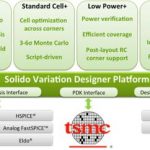
For a small company, Solido has some very large customers and partners, TSMC being on of them. Why? Because of the high yield and memory performance demand on leading edge technologies, that’s why.
Much has been made of and will continue to be said on the march of Moore’s Law. While economics of scale and performance vs. power… Read More
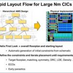
Ciranova presented a hierarchical custom layout flow used on several large advanced-node designs to reduce total layout time by about 50%. Ciranova itself does automated floorplanning and placement software with only limited routing; but since the first two constitute the majority of custom layout time, and strongly influence… Read More
Atrenta presented an update on the TSMC Soft IP Alliance Program at TSMC’s theater each day at DAC. Mike Gianfagna, Atrenta VP of Marketing, presented an introduction to SpyGlass, an overview of the program and a progress report. Dan Kochpatcharin, TSMC Deputy Director of IP Portfolio, was also there. Between Mike, Dan, and I there… Read More
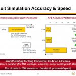
I caught the Berkeley Design Automation presentation in the TSMC Theater, where Simon Young (BDA’s director of product marketing) described the Analog FastSPICE (AFS) nanometer circuit verification platform, built on their foundation of very fast, very accurate, high capacity circuit simulation.
BDA claims the AFS platform… Read More
What a great interview! Xilinx CEO Moshe Gavrielov is right on the money HERE where he credits the high 28nm yields to the “very intimate” linkage in process development with TSMC.… Read More