You are currently viewing SemiWiki as a guest which gives you limited access to the site. To view blog comments and experience other SemiWiki features you must be a registered member. Registration is fast, simple, and absolutely free so please,
join our community today!
            WP_Term Object
(
    [term_id] => 24
    [name] => TSMC
    [slug] => tsmc
    [term_group] => 0
    [term_taxonomy_id] => 24
    [taxonomy] => category
    [description] =>
    [parent] => 158
    [count] => 585
    [filter] => raw
    [cat_ID] => 24
    [category_count] => 585
    [category_description] =>
    [cat_name] => TSMC
    [category_nicename] => tsmc
    [category_parent] => 158
    [is_post] =>
)

WP_Term Object
(
    [term_id] => 24
    [name] => TSMC
    [slug] => tsmc
    [term_group] => 0
    [term_taxonomy_id] => 24
    [taxonomy] => category
    [description] =>
    [parent] => 158
    [count] => 585
    [filter] => raw
    [cat_ID] => 24
    [category_count] => 585
    [category_description] =>
    [cat_name] => TSMC
    [category_nicename] => tsmc
    [category_parent] => 158
    [is_post] =>
)
3D-IC design has become a popular discussion topic in the past few years because of the integration benefits and potential cost savings, so I wanted to learn more about how the DRC and LVS flows were being adapted. My first stop was the Global Semiconductor Alliance web site where I found a presentation about how DRC and LVS flows were… Read More
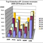
Is it surprising to see that Synopsys has been selected Interface IP partner of the year by TSMC? Not really, as the company is the clear leader on this IP market segment (which includes USB, PCI Express, SATA, DDRn, HDMI, MIPI and others protocols like Ethernet, DisplayPort, Hyper Transport, Infiniband, Serial RapidIO…). But,… Read More
Ever since the TSMC OIP Forum where Dr. Shang-Yi Chiang openly asked customers, “When do you want 3D Transistors (FinFETS)?” I have heard quite a few debates on the topic inside the top fabless semiconductor companies. The bottom line, in my expert opinion, is that TSMC will add FinFETS to the N20 (20nm) process node in parallel with… Read More
Hello Daniel,
I am very interested on the articles on the PVT simulation, I have worked in that area in the past when I worked in process technology development and spice modeling and I also started a company called Device modeling technology (DMT) which built a Spice model library of discrete components, such as Bipolar/MOS /POWER… Read More
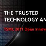
The TSMC OIP conference was Monday and Tuesday of last week. You have probably NOT read about it since it was invitation only and press was not invited. Slides were not made available (except for Mentor), no photos or video were allowed, it was a very private affair. Given that, I won’t be able to go into great detail but I will give you… Read More
EDA companies and foundries must closely collaborate in order to deliver IC tool flows that work without surprises at the 40nm and 28nm nodes.
Tomorrow in San Jose you can attend this 4th annual event hosted by TSMC along with Mentor Graphics and other EDA and IP companies.
Here are some of the topics that will interest IC designers… Read More
If you follow the SemiWiki Twitter feed you may have noticed that The Motley Fool (Seth Jayson) did three more articles on TSMC financials. The first Foolish article was blogged on SemiWiki as “TSMC Financial Status and OIP Update”.
The next three Fool Hardy articles look at cash flow (the cash moving in and out of a business), accounts… Read More
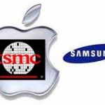
Apple will purchase close to eightBILLION dollars in parts from Samsung for the iSeries of products this year alone, making Apple Samsung’s largest customer. Samsung is also Apple’s largest competitor and TSMC’s most viable competitive foundry threat so it was no surprise to see Apple and TSMC team up on the next generations of… Read More
While I was in Taiwan last month battling a Super Typhoon, Morris Chang was in Silicon Valley picking up his IEEE Medal of Honor. Gordon Moore, Andrew Grove, and Robert Noyce all have medals. The other winners, including 10 Nobel prize recipients, are listed HERE. An updated wiki on Dr. Morris Chang is located HERE.
The 12+ hour plane… Read More
Whether you use a gate-first or gate-last High-k Metal Gate implementation, yield will be your #1 concern at 28nm, which makes variation analysis and verification a big challenge. One of the consulting projects I have been working on with the foundries and top fabless semiconductor companies is High-Sigma Monte Carlo (HSMC) … Read More