
The TSMC OIP conference was Monday and Tuesday of last week. You have probably NOT read about it since it was invitation only and press was not invited. Slides were not made available (except for Mentor), no photos or video were allowed, it was a very private affair. Given that, I won’t be able to go into great detail but I will give you the impression it left on me and I will share slides from the best vendor presentation given on the second day.

TSMC OIP day 1 was for ecosystem partners (EDA, IP, Design Services) and I would say there were about 200 of us. My badge was courtesy ofSolido Design (I do the foundry work for Solido). Presentations were made by Cliff Hou, Vice President of Design Enablement, and LC Lou, Senior Director of IP Development and a couple of other TSMC guys that I did not know. I have worked with both Cliff and LC over the years and have a great respect and trust for them.
28nm and 20nm were discussed in great detail in regards to design enablement and IP. It was very clear that TSMC is finished with 28nm which ramped 3 times faster than 40nm. All 28nm process nodes: 28HP, 28HPL, 28LP and 28HPM (M=mobile) are in production with thousands of wafers already shipped to customers. This tracks with what I have heard from TSMC’s top customers, 28nm silicon is out and working. The first 20nm production wafers are scheduled for mid 2012. This also tracks with what customers have told me, who are finishing up 20nm PDKS in time for Christmas.
The technical deep dive was on RDRs (restricted design rules) which are new in 28nm. TSMC said it took customers about a month to adjust to RDRs which may be a little optimistic. The 28nm DRM (design rule manual) is significantly larger than 40nm, meaning the rules are more difficult to describe. Feedback I got from customers however was that RDRs made their life easier and without RDRs 28nm would not have yielded well at all.
3D IC was discussed in great detail which is a blog in itself. The takeaway here is that TSMC is leading the way in 3D IC, believe it. The other interesting topic was LDEs (layout dependent effects). New effects are coming at 20nm so you can bet LDE will be a big part of the next round of TSMC reference flows (13.0) you will see at the 2012 Design Automation Conference in San Francisco. These reference flows will probably be at 20nm since DAC is mid 2012, same as TSMC 20nm availability. Early access to process technology by both partners and customers was mentioned throughout the two days and I can tell you TSMC is doing much better with early access than other foundries, which was a clear differentiator for the top fabless companies at 28nm.
Day 2 was for customers which I would guess was close to a thousand people. Rick Cassidy, President of TSMC North America, did the keynote. Side note: Rick is a West Point graduate which may explain his no nonsense speaking style. Shang-Yi was next then Cliff Hou. The hot topic here was FinFets. I have blogged about this before but the message that day was FinFets would have delayed 20nm so TSMC stuck with planar transistors. The FinFet design ecosystem challenge was discussed (3D extraxtion, modeling, etc…) and TSMC flat out asked customers if they wanted FinFets for 14nm (2015). The customers I talked to will look at the technical versus time-to-market trade-offs of FinFets which is still being calculated.
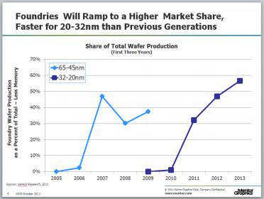
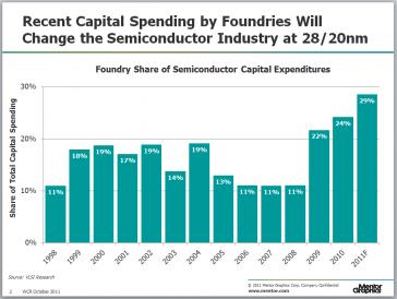
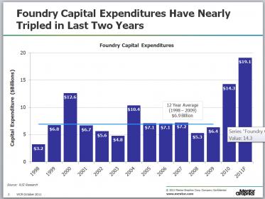
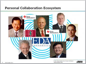
Vendor presentations were next from Mike Inglis (ARM), Aart de Geus (Synopsys), Lip-bu Tan (Cadence), and Wally Rhines (Mentor). Mentor was the only vendor “open enough” to send me slides so that is the only presentation I will mention. According to Wally 28/20nm will be a “Golden Era” for foundries. Massive capital investment by foundries will yield (pun intended) very cost effective wafers that will absorb existing products at the higher nodes. 28/20nm cost and capability will also drive new applications and accelerate semiconductor industry growth for years to come. Absolfreakinlutely!
Wally’s presentation has 45 slides and several important points which should be independent blogs. His last slide is my favorite however, it is his personal collaboration ecosystem. My personal collaboration ecosystem is much larger of course since it includes all of you.


Comments
0 Replies to “TSMC 2011 Open Innovation Platform Ecosystem Forum Trip Report”
You must register or log in to view/post comments.