Ever since the TSMC OIP Forum where Dr. Shang-Yi Chiang openly asked customers, “When do you want 3D Transistors (FinFETS)?” I have heard quite a few debates on the topic inside the top fabless semiconductor companies. The bottom line, in my expert opinion, is that TSMC will add FinFETS to the N20 (20nm) process node in parallel with planar transistors and here are the reasons why:

Eliminating EXCESS: In the next few years, traditional planar CMOS field-effect transistors will be replaced by alternate architectures that boost the gate’s control of the channel. The UTB SOI
The1999 IDM paper Sub 50-nm FinFET: PMOSstarted the 3D transistor ball rolling then in May of 2011 Intel announceda production version of a 3D transistor (TriGate) technology at 22nm. Intel is the leader in semiconductor process technologies so you can be sure that others will follow. Intel has a nice “History of the Transistor” backgrounder in case you are interested. Probably the most comprehensive article on the subject was just published by IEEE Spectrum “Transistor Wars: Rival architectures face off in a bid to keep Moore’s Law alive”. This is a must read for all of us semiconductor transistor laymen.

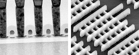
DOWN AND UP: A cross section of UTB SOI transistors and a micrograph of an array of FinFET transistors .
Why the push to 3D transistors at 20nm?
Reason #1 is because of scaling. From 40nm to 28nm we saw significant opportunities for a reduction in die size and power requirements plus an increase in performance. The TSMC 28nm gate-last HKMG node will go down in history as the most profitable node ever, believe it! Unfortunately standard planar transistors are not scaling well from 28nm to 20nm, causing a reduction of the power/die savings and performance boost customers have come to expect from a process shrink. From what I have heard it is half what was expected/hoped for. As a result, TSMC will definitely offer 3D transistors at the 20nm node, probably as a mid-life node booster.

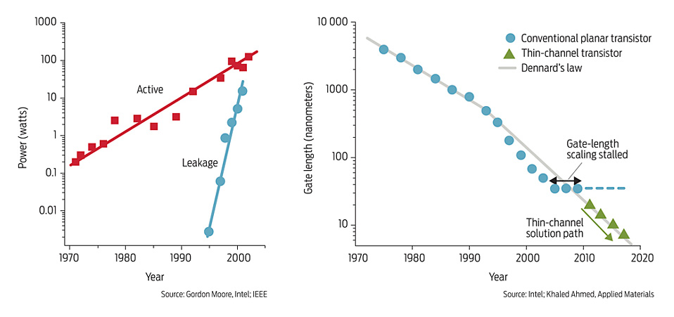
Shrinking returns: As transistors got smaller, their power demands grew. By 2001, the power that leaked through a transistor when it was off was fast approaching the amount of power needed to turn the transistor on , a warning sign for the chip industry. As these Intel data show, the leakage problem eventually put a halt to the transistor scaling , a progression called Dennard’s law. Switching to alternate architectures will allow chipmakers to shrink transistors again, boosting transistor density and performance.
Reason #2 is because TSMC can and it will offer a significant competitive advantage against the second source foundries (UMC, GFI, SMIC). DR. Chenming Hu is considered an expert on the subject and is currently a TSMC Distinguished Professor of Microelectronics at University of California, Berkeley. Prior to that he was the Chief Technology Officer of TSMC. Hu coined the term FinFET 10+ years ago when he and his team built the first FinFETs and described them in the 1999 IEDM paper. The name FinFET because the transistors (technically known as Field Effect Transistors) look like fins. Hu didn’t register patents on the design or manufacturing process to make it as widely available as possible and was confident the industry would adopt it. Well, he was absolutely right!
The push for 3D transistors clearly shows that the days of planar transistor scaling will soon be behind us. It also shows what lengths we will go through to continue Moore’s Law. Or as TSMC says “More-than Moore Technologies”.
Share this post via:


Comments
0 Replies to “3D Transistors @ TSMC 20nm!”
You must register or log in to view/post comments.