




Semiconductor manufacturing depends on lithography: the process of transferring tiny circuit patterns onto a silicon wafer. Conventional extreme-ultraviolet (EUV) lithography projects light with a wavelength of 13.5 nanometers through a reflective optical system, using a custom photomask to define each layer. It can … Read More

Author: Admin
Maskless EUV Lithography: An Alternative to E-Beam

Terafab’s Single Roof: Why Packaging, Not Lithography, Decides High Volume

By Shaurya Seth
Terafab is one of the most ambitious projects of the decade: $16.8 billion for phase one and up to $119 billion across four phases. A research fab in Austin iterates on process recipes, transistor designs, and packaging variants at a few thousand wafers per month. A volume fab in Grimes County targets 100,000 wafer… Read More
Why Semiconductor AI Starts with Data, Not Algorithms

The next gains from AI in semiconductors will come less from models and more from making fab and test data reliable, connected and tied to engineering decisions.
By Sriram Nithin Gopal Lanka
Every few months there is a new AI model that can do more and semiconductor manufacturers are under pressure to put them to work. But ask the engineers… Read More
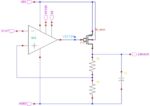
The silent killer of analog reliability: Why SPICE misses floating net
By Bhanu Pandey
The semiconductor industry is currently facing a significant challenge in functional verification. According to the most recent Wilson Research Group / Siemens EDA Functional Verification Study, first-silicon success rates have hit a historic low, with nearly 68% of designs requiring two or more spins. While… Read More
The Pivotal Moments That Gave Rise to Silicon Valley

The little-known decisions and breakthroughs—and the remarkable role of Robert Noyce—that helped shape the modern semiconductor industry
by Sunil Mehta
When people tell the story of how Silicon Valley came into being, they usually begin with a familiar sequence of events.
The transistor was invented at Bell Labs. William Shockley… Read More
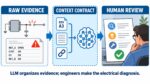
LLM-assisted schematic test-report analysis and root-cause investigation
By Piyush Bag
Intro: In this AI era, building data centers has become crucial not just for hyperscalers, but for many companies as well, as they build the infrastructure for AI. At a high level, a data center includes compute, storage, networking, and other infrastructure. This article is about the design lifecycle of network hardware.… Read More
SEMICON West’s “Bridging design and Manufacturing with AI” Design Session Explores AI as Practical Lever Across Entire Lifecycle

By Julie Rogers, Executive Director, Electronic System Design Alliance
SEMICON® West 2026 is “Bridging Design and Manufacturing with AI” during a day-long session Tuesday, October 13, from 10:30 a.m. to 4:30 p.m. at San Francisco’s Moscone Center, North Hall, Lower Level, Room 20.
The Design Session hosted and organized by … Read More
The Technical Problem Is Often Not the Business Problem

By Prof. Dr. S. Filo Ambrosini
On a semiconductor line, a rising defect rate can trigger a familiar debate. Do we need a new inspection system? More sensors? An additional engineer?
Those may all be valid responses. But before making the decision, someone needs to establish when the change began, where it first appears, and whether… Read More
A Study of Photoresist Bake Influence on Stochastics for DUV Immersion Lithography

Deep-ultraviolet (DUV) immersion lithography remains a critical patterning technology for advanced semiconductor manufacturing. Using a 193 nm ArF exposure system with water between the projection lens and wafer, immersion lithography increases numerical aperture and enables smaller features than dry exposure. However,… Read More
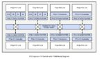
PCIe 7 Switch IP with Time Division Multiplexing: Powering the Next Generation of AI Connectivity
By Tim Messegee, Senior Director of Solutions Marketing at Rambus
PCI Express (PCIe), PCIe switches, Time Division Multiplexing (TDM), Network Interface Cards (NICs), and SmartNICs are all well-established technologies that have formed the backbone of computing and networking systems for years. More recently, SuperNICs… Read More






The $725 Million Chip Development: Why Execution Risk, Not IP Cost, Now Dictates Advanced-Node Survival