







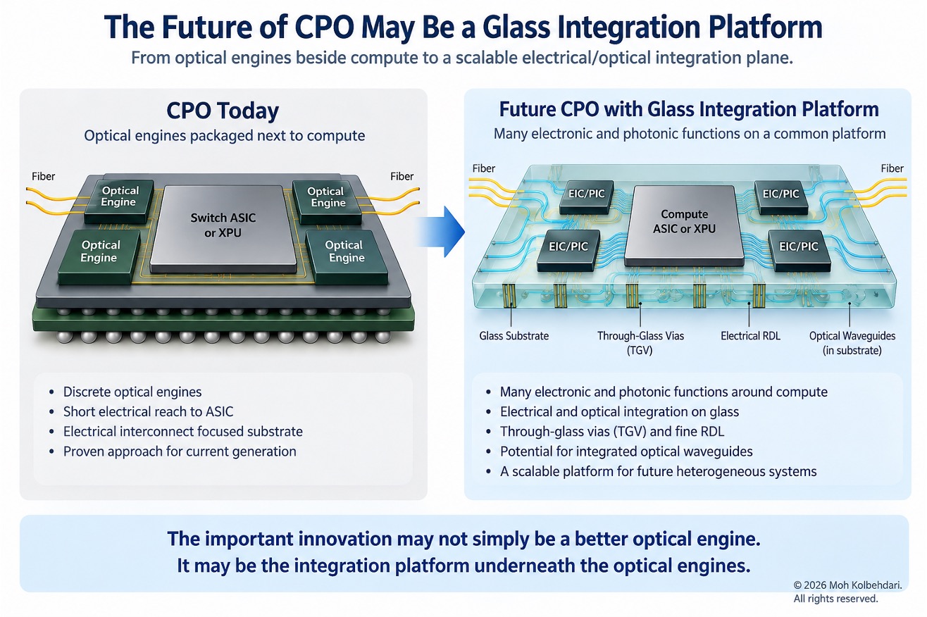
Co-packaged optics is usually described as a proximity problem.
Move the optical engine closer to the switch ASIC or XPU. Shorten the electrical path. Reduce SerDes power. Increase bandwidth density.
That direction is real.
Optical functionality is moving progressively closer to compute.
But proximity does not eliminate the physical problem.
A physical bottleneck rarely disappears; it changes coordinates across the system.
As electrical reach becomes shorter, greater responsibility moves into the package: substrate geometry, EIC/PIC integration, optical alignment, thermal and mechanical stability, manufacturing, test, and reliability.
That leads to a larger question.
What physical platform will allow increasingly diverse electrical and optical functions to coexist around very large compute devices?
One increasingly interesting answer may be glass.
The opportunity is larger than replacing an organic substrate or substituting glass for a silicon interposer.
Glass could eventually become a scalable heterogeneous-integration platform for electronic and photonic functions around compute.
That possibility deserves much more attention.
CPO Is Beginning to Challenge the Substrate
Today’s advanced AI packages already combine very different physical systems.
Large compute ASICs require enormous electrical connectivity and power delivery.
HBM adds density, thermal interaction, package size, and mechanical complexity.
Optical engines introduce EIC/PIC integration, optical coupling, fiber attachment, and extremely sensitive geometric relationships.
The substrate sits underneath all of them.
At some point, the substrate is no longer simply carrying the architecture.
It begins determining which architecture is physically practical.
This connects directly to a broader thesis I have discussed in earlier work:
The package is no longer merely supporting the system. It is defining what system can be built.
CPO pushes that idea further.
If the package determines whether compute, memory, electrical interconnect, optics, power, cooling, manufacturing, and test can coexist, then the substrate underneath that package becomes increasingly strategic.
The question is no longer simply:
Which optical engine should we use?
It becomes:
What integration platform can support the next generation of optical and electronic functions around compute?
Why Glass Becomes Interesting
Glass has several properties that make it attractive for this problem.
It can provide very good dimensional stability.
It can support low-loss high-frequency electrical routing.
Its smooth surface can support increasingly fine redistribution structures.
Its coefficient of thermal expansion can be engineered.
And unlike a conventional silicon interposer constrained by wafer geometry and economics, glass offers the possibility of considerably larger integration dimensions.
Those characteristics become especially interesting when optical integration enters the package.
Optical systems care deeply about geometry.
Electrical routing can tolerate certain variations that an optical interface may not.
Fiber attachment, couplers, waveguides, PIC placement, and optical alignment all become increasingly sensitive as integration density increases.
That means dimensional stability becomes more than a mechanical property.
It becomes an architectural capability.
The Substrate Could Eventually Participate in the Optical System
This is where the glass story becomes more interesting than a simple material substitution.
Today, we generally think of the package substrate as the electrical platform underneath the devices.
But future glass structures could potentially support both electrical and optical functions.
Electrical redistribution could occur laterally.
Through-glass vias could provide vertical connectivity.
And optical structures could eventually become part of the substrate environment itself.
That suggests a more important possibility:
The CPO substrate may eventually participate in both electrical and optical integration.
The substrate would no longer simply connect the optical engine to the ASIC.
It could become part of the physical environment through which multiple optical and electronic functions are integrated.
That changes the architectural role of the substrate.
Think Beyond One Optical Engine
Much of today’s CPO discussion still assumes a relatively simple picture:
one large switch ASIC,
surrounded by a number of optical engines,
with very short electrical connections between them.
That is an important architecture.
But it may not be the final one.
As bandwidth density increases, optical functionality could become more distributed.
Instead of a small number of relatively large optical engines, future systems may contain many smaller electronic and photonic functions positioned around compute.
That creates a different scaling problem.
The question becomes less about packaging an optical engine and more about creating a platform capable of supporting many optical and electronic functions simultaneously.
This is where glass could become especially interesting.
A sufficiently mature glass platform could potentially provide:
large integration area,
fine electrical redistribution,
stable geometry,
vertical connectivity,
and eventually optical routing.
The value proposition therefore becomes much larger than replacing one substrate material with another.
Glass could become an integration plane.
The Optical Function Is Not the Product
There is another important distinction.
The optical function is not the product.
A PIC can demonstrate excellent optical performance.
An optical engine can demonstrate very high bandwidth.
A glass substrate can demonstrate excellent electrical loss or dimensional stability.
None of those demonstrations alone establishes a scalable product.
The complete system still has to survive assembly, manufacturing variation, thermal cycling, mechanical stress, optical alignment, electrical interfaces, test, qualification, and production yield.
That is why the future of glass will not be determined simply by its material properties.
It will be determined by whether those properties can be converted into a repeatable manufacturing platform.
TGV Is One of the Critical Gates
One of the most important technologies in that transition is the through-glass via, or TGV.
Conceptually, a TGV is straightforward.
Create a vertical opening through glass and provide electrical connectivity through it.
Manufacturing it reliably at advanced-packaging scale is considerably harder.
The challenges include via geometry, glass damage, metallization, copper filling, interface adhesion, residual stress, cracking, and long-term reliability.
As feature dimensions become smaller and via counts become larger, those problems become increasingly important.
This is why the glass opportunity should not be evaluated only from a material-property table.
The important question is whether the industry can mature:
glass processing + TGV + fine RDL + assembly + reliability
into a repeatable manufacturing ecosystem.
That is the real transition.
Glass Is Not Automatically a Thermal Solution
There is also an important misconception to avoid.
Glass should not automatically be described as a superior thermal material.
It is not.
Glass does not inherently provide the heat-spreading capability of materials specifically selected for high thermal conductivity.
The opportunity is different.
Glass offers potential advantages in electrical behavior, dimensional stability, large-area scaling, and heterogeneous integration.
The thermal path must still be deliberately engineered through the full package.
That distinction matters because increasingly large AI packages cannot treat thermal design as a secondary concern.
The substrate can enable the architecture without being the primary heat-removal mechanism.
The Ecosystem May Matter More Than the First Demonstration
A successful demonstration does not create an industry platform.
An ecosystem does.
Glass-based integration will require compatible materials, process equipment, TGV manufacturing, fine-line redistribution, assembly methods, known-good-die strategies, inspection capability, qualification methods, and multiple manufacturing sources.
That ecosystem will take time to mature.
And this is another recurring semiconductor pattern.
The first demonstration proves possibility.
Manufacturing proves repeatability.
The ecosystem determines scale.
The most important milestone therefore may not be the first impressive glass package.
It may be the point when designers can select glass as an integration platform without treating every program as a custom research project.
That is when the technology becomes architectural.
The Bottleneck Changes Coordinates
This brings the discussion back to CPO.
CPO began because high-speed electrical reach was becoming increasingly expensive in power and increasingly difficult to scale.
Moving optical conversion closer to compute addresses part of that problem.
But:
A physical bottleneck rarely disappears; it changes coordinates across the system.
Shorter electrical reach places greater importance on optical alignment.
Closer optical integration increases thermal exposure.
Larger heterogeneous structures increase mechanical sensitivity.
More integrated architectures increase the importance of assembly, test, reliability, and manufacturing repeatability.
The bottleneck moves.
That is why CPO cannot ultimately be understood only as an optical-engine problem.
It is becoming an integration-platform problem.
From Substrate to Integration Plane
The most interesting question about glass may therefore not be:
Can glass replace organic substrates?
Or:
Can glass replace silicon interposers?
Those comparisons are useful, but they may be too narrow.
The more consequential question is:
Can glass become a scalable physical integration plane for many electronic and photonic functions around compute?
If TGV, fine redistribution, optical integration, assembly, and the supporting manufacturing ecosystem mature sufficiently, the answer could eventually be yes.
And if that happens, the substrate itself changes role.
It becomes part of the architecture.
That leads to the larger thesis:
The important innovation may not simply be a better optical engine. It may be the integration platform underneath the optical engines.
CPO began by moving optics closer to compute.
Its next chapter may be about building the physical platform that allows many optical and electronic functions to coexist around compute at scale.
Glass may become one of the technologies that makes that possible.
And if it does, the future of CPO will not simply be about packaging optics.
It will be about defining the physical platform on which the next heterogeneous compute system can be built.
Also Read:
Semiconductor Engineering Has a State-Continuity Problem
When Design Gets Faster, the Bottleneck Moves Through the Physical Stack
The Fab Is Not the Finish Line
Share this post via:



The silent killer of analog reliability: Why SPICE misses floating net