

Engineered substrate technology is driving an evolution within the semiconductor industry. As Moore’s Law reaches its limits, the focus is shifting from traditional planar wafer scaling to innovative material engineering and 3D integration. Companies like Soitec, Intel and Samsung are pioneering this transition, unlocking new levels of performance, efficiency, and scalability.
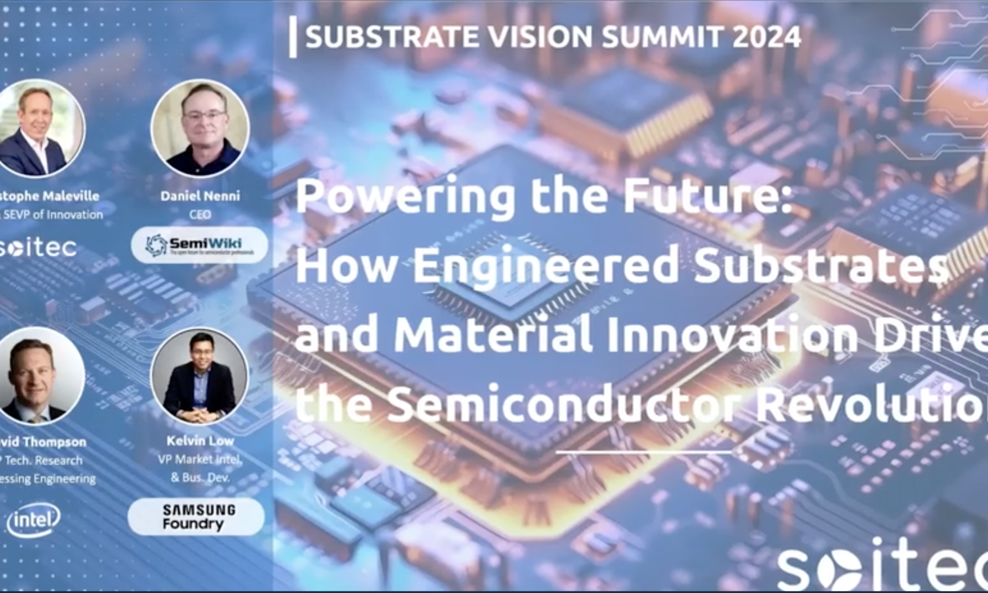
The topic of engineered substrates and material innovation was the focus of an interesting panel discussion at the Substrate Vision Summit 2025. Daniel Nenni, Founder of SemiWiki.com, moderated the session. SemiWiki.com is a popular online platform featuring an active discussion forum dedicated to semiconductors. Christophe Maleville, CTO & SEVP of Innovation at Soitec, David Thompson, VP Technology Research at Intel, and Kelvin Low, VP Market Intelligence & Business Development at Samsung Foundry, were the panelists.
Engineered Substrates: Changing the Competitive Landscape
One of the most compelling advantages of engineered substrates is the ability to preinstall critical performance elements into the wafer itself. By embedding functionality at the substrate level, chip designers can achieve significant improvements in efficiency and power savings.
A clear example of this was shown several years ago with RF-SOI wafers, where Soitec proved how a 2G design achieved 3G-level performance simply by switching to an RF-SOI wafer. This breakthrough provided GaAs-like performance without using GaAs technology, proving the potential of engineered wafers across various applications. Such advancements not only enhance performance but also accelerate product development cycles and reduce design complexity.
Addressing Challenges of Engineered Wafers
Semiconductor manufacturers face two major cost components: the cost of processing the wafer (internally or through procurement) and the cost of time (technology development cycles, learning curves, and integration challenges).
If every manufacturer were to independently develop SOI wafer technology, it would be an inefficient process with a steep learning curve. Instead, by relying on specialized providers like Soitec, foundries and chipmakers can source mature, high-performance engineered substrates and focus on differentiation at the chip level. This ecosystem-driven approach accelerates technology readiness and product development while ensuring cost efficiency.
Foundry Adoption and Market Demand
Foundries are recognizing the strategic importance of engineered substrates, particularly for Fully Depleted SOI (FD-SOI) technology. Samsung Foundry, a key player in this space, has already adopted 28FD-SOI in high-volume production at its Austin, TX fab, with customers like NXP and Lattice leveraging its benefits. Furthermore, Samsung is expanding its FD-SOI capacity to meet rising demand, while GlobalFoundries has also joined the ecosystem, reinforcing the technology’s viability. 18FD-SOI is on Samsung Foundry’s roadmap with ST Microelectronics as the lead customer.
Despite early concerns about cost and supply chain stability, FD-SOI has proven to be a compelling solution for applications that can manipulate body-biasing to achieve low power and high efficiency. Soitec has further addressed adoption challenges by investing in design infrastructure—including the acquisition of Dolphin Integration—to enhance support for SOI-based designs.
The 3D Future of Engineered Wafers
Both Soitec and Intel are embracing the 3D way of building engineered wafers. Soitec is advancing Smart Cut™ technology to enable precise layer transfer, facilitating hybrid bonding and wafer stacking for 3D integration. Intel, on the other hand, is developing Foveros 3D stacking, which enables transistors and logic units to be vertically integrated for improved performance and energy efficiency.
Unlike the traditional planar approach, where transistors are arranged side by side, the 3D method stacks layers vertically, reducing interconnect distances and power consumption. This shift is critical for sustaining Moore’s Law and ensuring future generations of semiconductors meet the growing demands of AI, high-performance computing, and edge applications.
Standardization and Scalability: Key to Mass Adoption
The conversation around wafer size standardization is evolving, but the real challenge lies in standardizing die-to-die interconnects for chiplet-based designs. UCIe (Universal Chiplet Interconnect Express) is leading this initiative, enabling interoperability across different foundries and manufacturers.
From an economic standpoint, scaling wafer size can yield more dies per wafer. For engineered materials like SiC or GaN, the cost-benefit analysis varies. A 300mm GaN substrate, for example, can achieve 20X Figure of Merit improvement over a 200mm GaN wafer, demonstrating the potential for engineered substrates to revolutionize power electronics and RF applications.
Value Creation Beyond Die Cost
Ultimately, the value of engineered substrates extends beyond raw die cost. By enhancing performance, reducing power consumption, and enabling new system architectures, these wafers deliver system-wide cost savings and new application possibilities. Without this broader perspective, certain technologies—such as SiC for power electronics—would struggle to establish a strong business case based solely on die cost.
Summary
As the semiconductor industry moves toward a 3D future, engineered substrates are becoming a strategic enabler of next-generation computing. Preinstalling critical performance elements into the wafer itself is helping redefine what’s possible in chip design. Foundries are embracing FD-SOI, and the push for larger, high-performance wafers is opening the door for more efficient, scalable, and cost-effective semiconductor manufacturing.
With increasing demand for AI, 5G, automotive, and high-performance computing, engineered substrates will be at the heart of the semiconductor industry’s next wave of innovation. The companies that leverage this technology early will be the ones shaping the future of computing.
Also Read:
Soitec: Materializing Future Innovations in Semiconductors
I will see you at the Substrate Vision Summit in Santa Clara
EVs, Silicon Carbide & Soitec’s SmartSiC™: The High-Tech Spark Driving the Future (with a Twist!)
Share this post via:


Comments
There are no comments yet.
You must register or log in to view/post comments.