Designers require comprehensive logical, physical, and electrical models to interpret the results of full-chip power noise and electromigration analysis flows, and subsequently deduce the appropriate design updates to address any analysis issues. These models include: LEF, DEF, Liberty library models (including detailed CCS-based behavior), SPEF/DSPF, VCD/FSDB, etc. – the size of the complete chip dataset for analytics in current process nodes could easily exceed 3TB. Thus, the power distribution network (PDN) analysis for I*R voltage drop and current densities needs to be partitioned across computation cores.
Further, the simulation vector-based analysis (of multiple operating scenarios) to evaluate dynamic voltage drop (DvD) necessitates high throughput. As a result, elastically scalable computation across a large number of (multi-core) servers is required. Two years ago, ANSYS addressed the demand for computational resource associated with very large multiphysics simulation problems with the announcement of their SeaScape architecture (link).
Some Background on Big Data
Big data is used to:
- Drive search engines, such as Google Search.
- Drive recommendation engines, such as Amazon and Netflix (“you might like this movie”).
- Drive real-time analytics, like Twitter’s “what’s trending”.
- Significantly reduce storage costs — e.g. MapR’s NFS compliant “Big Data” storage system.
Big data systems require a key new concept. Keep all available data, as you never know what questions you’ll later ask. All big data systems share these common traits:
- Data is broken into many small pieces called “shards”.
- Shards are stored and distributed across many smaller cheap disks.
- These cheap disks exist on cheap Linux machines. (Cheap == low memory, consumer-grade disks and CPU’s.)
- Shards can be stored redundantly across multiple disks, to build resiliency. (Cheap disks and cheap computers have higher failure rates.)
Big Data software (like Hadoop) use simple, powerful techniques so the data and compute are massively parallel.
- MapReduce is used to take any serial algorithm and make it massively parallel. (see Footnote [1])
- In-memory caching of data is used to make iterative algorithms fast.
- Machine learning packages run natively on these architectures. (see MLlib, http://spark.apache.org/mllib)
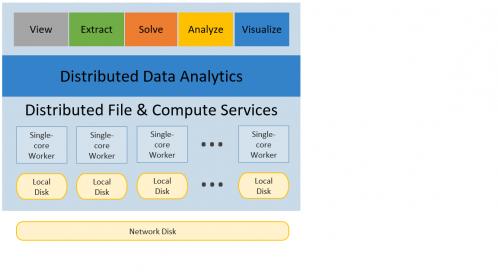
ANSYS SeaScape is modeled after the same big data architectures used in today’s internet operations, but purpose-built for EDA. It allows large amounts of data to be efficiently processed across thousands of cores and machines, delivering the ability to scale linearly in capacity and performance.
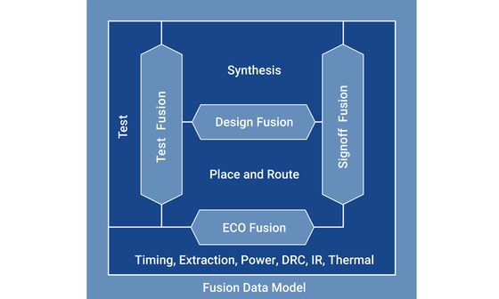
Simulation of advanced sub-16nm SoCs generates vast amounts of data. Engineers need to be able to ask interesting questions to perform meaningful analyses to help achieve superior yield, higher performance, lower cost – with the most optimum metallization and decap resources. The primary purpose of big data analytics is not simply to have access to huge databases of different kinds of data. It is to enable decisions based on that data relevant to the task at hand, and to do so in a short enough time that engineers can take action to adjust choices while the design is evolving. The SeaScape architecture enables this analytics capability (see the figure below).
RedHawk-SC
The market-leading ANSYS RedHawk toolset for power noise and EM analysis was adapted to utilize the SeaScape architecture – the RedHawk-SC product was announced last year.
I recently had the opportunity to chat with Scott Johnson, Principal Technical Product Manager for RedHawk-SC in the Semiconductor Business Unit of ANSYS, about the unique ways that customers are leveraging the capacity and throughput of RedHawk-SC, as well as recent features that provide powerful analytic methods to interpret the RedHawk-SC results to provide insights into subsequent design optimizations.
“How are customers applying the capabilities of RedHawk-SC and SeaScape?” I asked.
Scott replied, “Here are two examples. One customer took a very unique approach toward PDN optimization. Traditionally, P/G grids are designed conservatively(prior to physical design), to ensure sufficient DvD margins, with pessimistic assumptions about cell instance placement and switching activity. This customer adopted an aggressive ‘thin’ grid design, expecting violations to be reported after EM and DvD analysis – leveraging the throughput available, the customer incorporated iterations of RedHawk-SC into their P&R flow. A set of four ECO operations was defined, to address different classes of analysis issues. The ECO’s were applied in the P&R platform, and RedHawk-SC analysis was re-run. Blocks converged within two or three ECO + RedHawk-SC iterations – on average, the customer calculated they saved 7% in block area, as a result. And, this was all automatic, scripted into the P&R flow, no manual intervention required.”
“The second customer took a different, highly unique approach toward analytics of RedHawk-SC results. The SeaScape architecture inherently supports(and ships with) a machine learning toolset. The customer had been utilizing senior designers to review EM results, and make a binary fix or waive decision on high EM fail rate segments. The customer implemented an EMWaiver ML application on the SeaScape platform – after training, EMWaiver is presented with the EM results, and its inference engine automatically evaluates the fix-waive decision.” Scott continued.
Illustration of the EM Assistant application, using the ML features of SeaScape
Scott highlighted that as part of the training process, the precision and accuracy of the ML-based flow was assessed. The precision relates to the inferred “fix” designation that could have been waived, requiring additional physical design engineering resource – a precision factor of ~90% was reported (implying ~10% extra fixes). The accuracy relates to the risk of an inferred “waive” that actually requires a fix – the customer was achieving 100% accuracy, as required (i.e., no “escapes”).
“Sounds pretty advanced”, I interjected. “How would new customers leverage the model information and analytics detail available, after executing RedHawk-SC?”
Scott replied, “We have added a MapReduce Wizard interface in RedHawk-SC. Users progress through a series of menus, to select the specific design attributes of interest – e.g., cell type, cell instances, die area region – followed by the electrical characteristics of interest – e.g., cell loading, cell toggle rate, perhaps specific to cell in the clock trees.”
The figures below illustrate the steps through the RedHawk-SC MapReduce Wizard, starting with the selection of the design model view, and then the specific electrical analysis results of interest.
RedHawk-SC MapReduce Wizard menus for analytics – model data selection
MapReduce Wizard electrical analytics selection — e.g., power, current, voltage
“The MapReduce functional code is automatically generated, and applied to the distributed database.” , Scott continued. “An additional visualization feature in RedHawk-SC creates a heatmap of the analytics data, which is then communicated back to the user client desktop. Design optimizations can then quickly be identified – if a different analytics view is required, no problem. A new view can be derived on a full-chip model within a couple of minutes. Multiple visual heatmaps can be readily compared, offering an efficient multi-variable analysis of general complexity.”
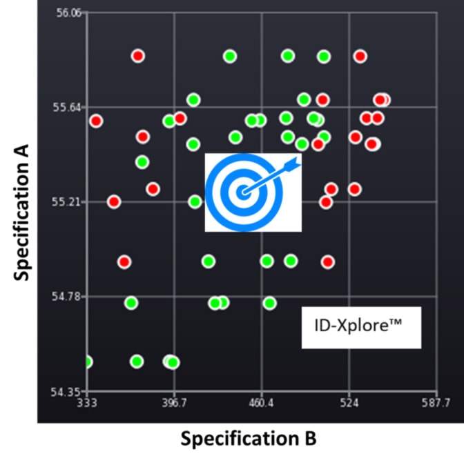
An example of a heatmap graphic derived from the analytics data is depicted below – this design view in this example selected clock tree cells.
Scott added, “In addition to these user-driven analytics, there is a library provided with a wealth of existing scenarios. And, the generated MapReduce code is available in clear text, for users to review and adapt.”
I mentioned to Scott, “At the recent DAC conference there was a lot of buzz about executing EDA tools in the cloud. The underlying SeaScape architecture enables a very high number of workers to be applied to the task. Is RedHawk-SC cloud-ready?”
Scott replied, “SeaScape was developed with the explicit support to run on the cloud. It’s more than cloud-ready – we have customers in production use on a(well-known)public cloud.”
“The level of physical and electrical model detail required for analysis of 5nm and 3nm process node designs will result in chip databases exceeding 10TB, perhaps approaching 20TB. Design and IT teams will need to quickly adapt to distributed compute resources and elastic job management like SeaScape, whether part of an internal or public cloud.”, Scott forecasted.
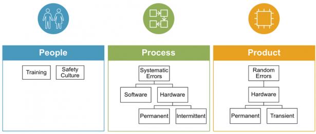
The computational resources needed to analyze full-chip designs have led to the evolution of multi-threaded and distributed algorithms and data models. The ability to efficiently identify the design fixes to address analysis issues has traditionally been a difficult task – working through reports of analysis flow results is simply no longer feasible. Analytics applied to a chip model consisting of a full set of logical, physical, and electrical data is needed. (Consider the relatively simple case of a library cell design that correlates highly to DvD or EM issues – how to quickly identify the cell as appropriate for a “don’t_use” designation required big data analytic information).
The combination of the SeaScape architecture with the features of ANSYS analysis and simulation products addresses this need. For more information on RedHawk-SC, please follow this link.
-chipguy
PS. Thanks to Annapoorna Krishnaswamy of ANSYS for the background material on Big Data applications and the ANSYS SeaScape architecture.
Footnote
[1] Briefly, MapReduce refers to the functional programming model that has been widely deployed as part of the processing of queries on very large databases – both Google and the Hadoop developers have published extensively on the MapReduce programming model. The “Map” step involves passing a user function to operate on (a list of) data shards, the same function executing on all workers. The result of executing the Map step is another list, where each entry is assigned a specific “key”, with an associated data structure filled with values. A simple example would be a text file parser function, where the keys are the “tokens” generated by the parser, and the data value is a count of the number of instances of that token (calling a “compress” or “combine” function after individual token parsing).
The next step is to “shuffle” the (key, value) records from the Map step, to assign the records to the specific “Reduce” node allocated to work on the key. All the records from each Map node for the key are sent to the designated Reduce node. As with the Map(function) step, a Reduce(function) step is then executed – Reduce is often referred to as the “aggregation” step. Again using a text parser as the example, the Reduce function could be a sum of the count values received from all the Map nodes for the key, providing the total instance count for each individual token throughout the input text file.
Overview of MapReduce
Illustration of the MapReduce architecture used by Hadoop
The data analytics features in SeaScape are based on the MapReduce programming model. An excellent introduction to MapReduce is available here.