webinar banner AI 2026 v2

Turnkey 2.5D HBM2 Custom SoC SiP Solution for Deep Learning and Networking Applications

Turnkey 2.5D HBM2 Custom SoC SiP Solution for Deep Learning and Networking Applications
by Daniel Nenni on 09-07-2018 at 7:00 am

Before we jump into the specifics, let us understand what’s driving custom solutions in the high performance computing and networking space. It’s the growing demand for core capacity and greater performance, which is due to the increase in the level of parallelism and multitasking required to handle the enormous amount of data traffic. According to market research, the increase in the core capacity has gone up from just a few cores to nearly 60+ cores. The memory and network bandwidth requirements will, by default, increase to keep pace with the increase in the core capacity and performance. As per the market research, the increase in the memory bandwidth has increased from 10Gbytes to roughly 400Gbytes, and the increase in the network IP traffic has gone up from 90 Exabytes to close to 300 Exabytes.

HIGH BANDWIDTH MEMORY (HBM2) CONTROLLER AND PHY

All these factors are pushing the need for custom processors, custom SoCs and specialized memories, like HBM, in the high performance computing and networking market segments. There are several high performance applications that demand high bandwidth memory access. Some examples are data center, networking, artificial intelligence, augmented reality and virtual reality, cloud computing, neural networks and several other high end applications. An HBM solution is ideas for these applications for three key reasons:

[LIST=1]

  • It currently supports a huge bandwidth of up 256GBps
  • It improves the power efficiency per pin
  • It offers a massive reduction in space, resulting in a form factor reduction of the end productOpen-Silicon’s first HBM2 IP subsystem in 16FF+ is silicon-proven at 2Gbps data rate, achieving bandwidths up to 256GBps, and being deployed in many customs SoCs. However, the data-hungry, multicore processing units needed for machine learning require even greater memory bandwidth to feed the processing cores with data. Keeping pace with the ecosystem, Open-Silicon’s next generation HBM2 IP subsystem is ahead of the curve with 2.4Gbps in 16FFC, achieving bandwidths up to >300GBps.

    This 7nm custom SoC platform is based on a PPA-optimized HBM2 IP subsystem supporting 3.2Gbps and beyond data rates, achieving bandwidths up to >400GBps. It supports JEDEC HBM2.x and includes a combo PHY that will support both JEDEC standard HBM2 and non-JEDEC standard low latency HBM. High speed SerDes IP subsystems (112G and 56G SerDes) enable extremely high port density for switching and routing applications, and high bandwidth inter-node connections in deep learning and networking applications. The DSP subsystem is responsible for detecting and classifying camera images in real time. Video frames or images are captured in real time and stored in HBM, then processed and classified by the DSP subsystem using the pre-trained DNN network.

    One application that goes hand-in-hand with high performance computing is AI. AI is revolutionizing and transforming virtually every industry in the digital world. Advances in computing power and deep learning have enabled AI to reach a tipping point toward major disruption and rapid advancement. Custom SoC platforms enable AI applications through training in deep learning and high speed inter-node connectivity, by deploying high speed SerDes, a deep neural network DSP engine, and a high speed high bandwidth memory interface with High Bandwidth Memory (HBM) within a 2.5D system-in-package (SiP). Open-Silicon’s implementation of a silicon-proven system custom SoC platform is centrally located within this ecosystem.

    About Open-Silicon
    Open-Silicon is a system-optimized ASIC solution provider that innovates at every stage of design to deliver fully tested IP, silicon and platforms. To learn more, please visit www.open-silicon.com


A Fresh Idea in Differential Energy Analysis

A Fresh Idea in Differential Energy Analysis
by Bernard Murphy on 09-06-2018 at 7:00 am

When I posted earlier on Qualcomm presenting with ANSYS on differential energy analysis, I assumed this was just the usual story on RTL power estimation being more accurate for relative estimation between different implementations. I sold them short. This turned out to be a much more interesting methodology for optimizing total energy using ANSYS PowerArtist.

Yadong Wang of Qualcomm presented and owns power modeling and analysis for Adreno GPUs. Before that he was a hardware power engineer in NVIDIA so he’s pretty experienced in this domain. He started by noting that the impact of power on heating is a big challenge in mobile GPUs. As you play a game on your phone, the temperature rises. Eventually thermal mitigation kicks in and clock speed drops; the game runs slower. The longer you play, the slower the game runs (down to some limit), which doesn’t make for great customer satisfaction. This is why thermal-constrained performance is becoming one of most important KPIs in mobile design.

This is a dynamic power problem. Assuming you’ve done all you can to minimize leakage (through process selection and power islands), and you accept you want to avoid switching to lower voltage/frequency options for the reason cited above, you really have to direct most of your attention to minimizing redundant activity, which you pretty much have to do at RTL. This is the low-cost place to perform design changes, you can iterate quickly on different options and the impact of changes is generally much higher than for any fixes that are practically possible at implementation. Yadong uses ANSYS PowerArtist in his work.

The common approach to optimizing power in these cases is run an analysis with some workload, look at the hierarchical breakdown of dynamic power components (switching power and internal power) through the design then look for cases where there might be redundant activity, such as a clock toggling on a register when the data input to that register isn’t changing. This process works but it doesn’t necessarily feel optimal. Maybe power savings may not be possible, but you might not know that until you’ve done quite a bit of searching. Wouldn’t it be better to know at the outset if there is opportunity to reduce power on this function and that the potential for reduction is significant? That’s where Qualcomm’s approach is really clever.

The core of the method looks at energy (power integrated over time) rather than power. And instead of hunting for redundant toggles, the method tweaks the workload (my view) by inserting bubbles in the path of incoming transitions or outgoing responses, to mimic starvation or stalls. This draws out the simulated time for that workload and therefore the time over which power is integrated to yield total energy.

Now they compare that energy report with the same report from a bubble-free run. The bubble-free case runs for less time with a higher average power, while the bubbled case runs for a longer time with lower average power. Ideally, total energy for these cases should be identical. But if there is power inefficiency in the design, the longer run-time in the bubbled case will amplify that inefficiency. So you know up-front whether there is opportunity to reduce total energy and you also have an idea of how much reduction may be possible.

Yadong took this further. In the experiments he described, he looked particularly at register-related dynamic power. Power estimation tools report switching and internal power separately; He noted that redundant D/Q toggles on a register will, in the bubbled case, cause an increase in both switching and internal energy, whereas redundant toggles on the clock input will increase only internal energy. Thus in comparison with the un-bubbled analysis there are 4 possibilities:

  • No change in switching or internal energy – no improvements are possible
  • Internal energy increases but switching energy is the same – there are redundant toggles on clock pins
  • Switching energy increases but internal energy is the same – there are redundant toggles on D/Q pins when the clock is disabled
  • Both switching energy and internal energy increase – there are redundant toggles on both D/Q and clock pins

They can drill down through detailed reports to find where they can make improvements to reduce redundant toggles.

What is especially startling is that Yadong said they were able to reduce dynamic power by 10% driven by this analysis. This is in a company (and a market) where reducing power is pretty close to a religion. But I’m not surprised the approach is so effective. This feels like a more scientific technique to measure power inefficiency overall and to isolate root causes. By comparison, traditional methods look rather ad-hoc.

Yadong mentioned at the end that a similar approach could be used to look at inefficiencies in memory, combinational logic and clock tree dynamic power. Analysis could pull similar data from the power estimation reports, though discriminating on differences in switching versus internal power might look different in each case. The Webinar is well worth watching. You can register to see it HERE.


Accelerating Design and Manufacturing at the 25th Annual IEEE Electronic Design Process Symposium

Accelerating Design and Manufacturing at the 25th Annual IEEE Electronic Design Process Symposium
by Camille Kokozaki on 09-05-2018 at 12:00 pm

25th annual IEEE Electronic Design Process Symposium
Accelerating Design and Manufacturing
September 13 & 14, 2018, SEMI, 673 S. Milpitas Blvd, Milpitas, CA 95035

This year marks a milestone in EDPS’s history as it turns 25. The event will be held at SEMI’s new headquarter facility and will provide a forum for EDA, foundry and design industries to address design and manufacturing issues. The Symposium will focus on acceleration methods for the design and manufacturing processes.

Key changes in designs and design methodologies continue to be an EDPS focus. Leading industry members will be sharing their challenges and solutions in this vibrant symposium. Real design in a real conversation setting will be discussed. EDPS 2018 sessions are based on the following themes:

  • Cyber Systems Design with emphasis on security
  • Innovative Designs and Design Techniques including Machine Learning in System Design and EDA
  • Smart Manufacturing – Increased cooperation between design & manufacturing (2.5/3D-IC Assembly and Test, Die-Pkg-Board CO-design flow, Flexible Hybrid Electronic)
  • System reliability with a special focus on ADAS, 5G, and Photonics.

The event will conclude with a panel discussion to analyze Blockchain’s role in EDA and Design. The Thursday evening banquet is co-located with the ESDA event “Building Start-Ups to Successful Exit” moderated by Jim Hogan.

Other Keynote Speakers include Chris Rowen, (CEO, BabbLabs) with an address entitled ‘Deep Learning Revolution – From Theory to Impact’. Andrew Kahng (Prof Computer Science & Engineering, UCSD) discussing ‘Evolutions of EDA, Manufacturing, and Design’. Simon Johnson (Sr Principal Engineer, Intel) will outline ‘Hardware-Based Security’.

Visit http://edpsieee.ieeesiliconvalley.org/ for additional details.

This event will offer time for Q&A after every presentation and plenty of networking time among ~ 100 attendees and speakers.

The event is sponsored by IEEE’s Council on Electronic Design Automation (CEDA) and Silicon Valley’s IEEE Computer Society and corporate Sponsors Ansys, Mentor Graphics, Intel with Semi as Associate Sponsor and IEEE’s Electronics Packaging Society as technical co-sponsor

In case you missed the early bird registration, EDPS is happy to offer a promo code “chipexpert-edps” that will provide $50 off the registration.You can register at edps2018.eventbrite.com and a complete schedule is available at ieee-edps.org and is attached here.

About EDPS:
The 2018 Electronic Design Process Symposium is the leading forum for advanced chip and systems development and CAD methodologies. As we approach the end of Moore’s law scaling, innovative packaging techniques are becoming increasingly important as package, board and other system components drive significant cost reduction. Innovative and smart manufacturing methodologies and flows are also becoming increasingly important. Since algorithmic development is changing rapidly, smart manufacturing enabling reduced NRE and faster time to market are critical.

Among other things, data center applications require heightened cybersecurity. 3DIC chip stacking of host processor and accelerator avoids exposing the bus between them to cyber-attacks. Implementation of machine and deep learning algorithms provide a higher level of defense against hacking. Cybersecurity is also very critical in system designs such as the ones found in automotive applications.

Reliability at the system level as well as at the package and chip level is impacted by ESD and thermal issues. Guaranteed performance needs to take aging and power into account. Newer interconnect, changing communication protocols and a wide range of operating conditions for systems require enhanced reliability for power and signal interconnects.

Heterogeneous integration of chips in high-performance processes and chips in mature process nodes allows higher performance and better yield optimization. More flexible system level partitioning will lead the way to new products’ development. Architectural modularity and IP re-use will enable higher performance at lower total system cost. New FPGA methodologies, especially embedded FPGA will see extensive use.

And last but not the least, machine learning is permeating all fields of system design and design tools.

A Trip Down Memory Lane:

The picture is of SemiWiki founder Daniel Nenni at the 2015 EDPS in Monterey:

The first session was chaired by Daniel Nenni and is on FinFET vs FD-SOI. It kicked off with a keynote from Tom Dillinger of Oracle (think Sun) followed by a panel session with Tom, Kelvin Low of Samsung Foundry, Boris Murman of Stanford University, Marco Brambilla of Synapse Design, and Jamie Shaeffer of GlobalFoundries:

The emergence of multiple transistor technology options at today’s deep submicron process nodes introduces a variety of power, performance, and area tradeoffs. This session will start with an overview of the FinFET and Fully-Depleted Silicon-on-Insulator devices (FD-SOI, also known as Ultra-Thin-Body SOI), in comparison to traditional bulk planar transistor technology. The session will then delve into a detailed discussion of the architectural and circuit implementation tradeoffs of these new offerings, to assist designers to make the right choice for their target application.

Detailed 2018 Program Info:


Unhackable Product Claims are a Fiasco Waiting to Happen

Unhackable Product Claims are a Fiasco Waiting to Happen
by Matthew Rosenquist on 09-05-2018 at 7:00 am

Those who think that that technology can be made ‘unhackable’, don’t comprehend the overall challenges and likely don’t understand what ‘hacked’ means.

Trust is the currency of security. We all want our technology to be dependable, easy to use, and secure. It is important to understand both the benefits and risks as we embrace new features and capabilities. For product companies, there is a challenge to show how their wares are desirable and differentiated from others. However, marketing claims around security can potentially undermine customer confidence, enrage potential attackers, and be a source of embarrassment.


The latest ‘unhackable’ tech marketing claim, for a digital wallet no less, falls after just a week. Luckily, it was an ethical hacker who disclosed their findings and not a cybercriminal who would have concealed the capability until such time as they could victimize users for their financial gain. There are many lessons to be learned.

Here are my top 4 tips for avoiding the pitfalls of overstating product security:

Rule #1: Never let marketing make promises (or guarantees) that products are “secure” “unbreakable” or ‘unhackable” when talking about the security of products. These words are absolutes for a domain where it is not possible. If there is a security story to be told, be cautious, accurate, and specific. It is far too easy to self-sabotage customer trust by flagrantly throwing about promises that can’t be kept or worse, quickly disproven. It makes confidence look like arrogance, deceit, or ignorance. To put this into rational terms of how momentously bad this is, I am not aware of any digital technology ever deployed into the real world for widespread use that is ‘unbreakable’. Do you really believe yours is the first? Don’t let hubris be your downfall.

Rule #2: It is important to understand how secure and resistant to attack your product is, but it requires a comprehensive evaluation and expert opinions. Security technologists (engineers, architects, coders, etc.) have different perspectives than security risk experts (threats, intelligence, methods, likelihood & impact calculations, etc.). Both are needed to understand the whole picture.

I would venture a guess, that in the case above, the security technologists likely stated all known vulnerabilities were closed, which was interpreted by marketing or management as their product was bullet-proof, while the security risk expert group was likely ignored or never engaged. Risk intelligence professionals would have outlined the types of threats most motivated, the objectives they would pursue, the likely methods employed, and what resources it would take to break the fundamental chains of trust.

Both disciplines, technical and intelligence, are needed when determining resistance, translating viewpoints, and comprehending risk. Don’t rely solely on a technical vulnerability scan or code audit to determine risk, as it is simply one facet of a complex model and only provides a partial overall outlook.

Rule #3: Never ignore how technology will be used, by whom, and what dependencies exist (network, supply chain, endpoint configuration, etc.). Anything is fair game, including the technology, processes, and people involved in the development, implementation, use, and sustaining support. Attackers don’t follow your product manual rules. They will be creative in finding the easiest way to exploit your products, likely in ways you didn’t consider.

Rule #4: Be kind to the white-hat hackers (i.e. security researchers) as they will work with you to make your products better. Save your venom for the cybercriminals and black-hat hackers who are agreeable with making your customers, their victims.

Moving forward
Trust is key for adopting technology. As the saying goes: “Trust is earned in drips and lost in buckets”. Choose your path, messages, and partners carefully.

Interested in more insights, rants, industry news and experiences? Follow me on your favorite social sites for insights and what is going on in cybersecurity: LinkedIn, Twitter (@Matt_Rosenquist), YouTube, Information Security Strategy blog, Medium, and Steemit


USB 3.x IP Revenue Have Grown by 31% in 2017 (IPnest)

USB 3.x IP Revenue Have Grown by 31% in 2017 (IPnest)
by Eric Esteve on 09-04-2018 at 12:00 pm

Despite the strong consolidation in the semiconductor industry, the Design IP market is going well, very well with YoY growth of 12%+ in 2017, according with the “Design IP Report” from IPnest. If we look at the Interface IP category (20% growth in 2017) and analyze the IP revenues by protocols, we can see that USB IP is amazingly healthy, showing a 31% YoY growth for USB 3.x IP. It’s amazing because the USB protocol was first released in the 1990’s and USB 3.0 in 2008.


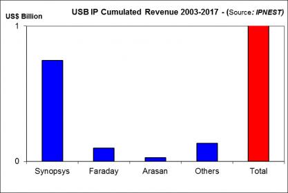
If you look at the above picture, you realize that USB protocol (USB 3.x, USB 2 and before) has generated 1 billion of IP revenues since 2003. Ipnest is closely following the wired interface IP category since 2008, I can confirm that USB IP yearly revenues have grown every year since 2003, again in 2017 and the 5 years forecast (2017-2022) is also exhibiting YoY growth. If you consider USB 3.x only, the attached 5 year CAGR is similar to the other protocols like PCIe, memory controller, MIPI or Ethernet, in the mid-ten points of percentage.

Now, if you integrate all the USB functions like USB 2 and below, the overal USB IP revenue is higher by 40%, but the growth rate lower. In fact, IPnest has splitted USB 3.x and USB 2 IP business since the begining in order to provide more accurate analysis. These two families have a different behavior, addressing different type of application. This split is unique if you consider the various wired interface protocols. Taking PCI Express as an example, when the version 2 was released, the chip makers who adopted PCIe 1.0 decided to move to PCIe 2.0 with no exception, the same again for the release 3.

If we consider USB adoption, the behavior is completely different in respect from USB 3.0 adoption. In many application integrating USB, the need was for a standard interconnect technology, allowing to plug and play with no burden, not for always more bandwidth capacity (like for PCIe). We have separately monitored USB 2 and USB 3.x IP revenues since 2008, and we can confirm that USB 2 IP revenues have grown up to 2014, althought USB 3.0 has been released in 2008. In 2017, the trend is clear, USB 2 is declining with revenues 30% lower than in 2013, when USB 3.x is growing, with IP revenue almost reaching $100 million and 31% YoY growth.


For every protocol, IPnest build 5 years forecast, like you can see on the above picture (except for USB, where we build two distinct forecast). To build a forecast, the analyst has two options. The first is to be an excellent Excel user, introduce a certain equation, and delegate your intelligence to the tool. That’s why you frequently see this type of forecast result: “$2142.24 million in 2027, with 23.45% CAGR” …

As far as I understand, the author thinks “the most digits after the comma, the best the forecast”.

The other option gives less impressive results, but hopefully more accurate. In fact, you need to consider all the parameters that make sense in our industry. Like the market trends by segment (data center, storage, PC, PC peripherals, mobile, wired networking, wireless networking and so on). You need to evaluate the number of designs starts where the protocol will be integrated, and the target technology node (if you look at the above picture, we have evaluated this number to be 500 in 2020 for USB 3.x. They can’t be all on 7nm, right?). You also need to have an accurate idea of the average license pricing, for the digital part (the controller) and for the PHY. Moreover, you need to be accurate when forecasting this license ASP over 5 years.

At this stage, forget that you may have learned during your MBA, the wired protocol license ASP is GROWING, not declining with time (like commodity pricing would do).

At the end, you may use Excel, in fact you need to, but the best tool, by far, is your market intelligence and your experience in the semiconductor business (I have started in 1983, have seen many downturns, bubbles and heard enough stupid statement to stay reasonable…).

I must confess that IPnest has an advantage over the competition in term of forecast. Because we have started in 2009, we can confront a forecast made in 2010 with actual results 5 years later! And the difference is below 10%, and sometimes even below 5%…

The next picture shows that I am very proud to be part of the DAC IP committee (since 2016), where I really enjoy to discuss with other IP experts and confront our ideas. By the way, last DAC was great, and we have seen that the booths left empty by the lack of EDA start-up have been filled by IP start-up!

I will propose later in September a detailed analysis for another protocol (PCIe? Memory controller? Very High Speed SerDes?… you may suggest which one in a comment). If you’re interested by the complete analysis of the wired interface IP market and 5 years forecast, the “Interface IP Report” will be released at the end of September, just contact me: eric.esteve@ip-nest.com .

Eric Esteve from IPnest


The Ever-Changing ASIC Business

The Ever-Changing ASIC Business
by Daniel Nenni on 09-04-2018 at 7:00 am

The cell-based ASIC business that we know today was born in the early 1980s and was pioneered by companies like LSI Logic and VLSI Technology. Some of this history is covered in Chapter 2 of our book, “Fabless: The Transformation of the Semiconductor Industry”. The ASIC business truly changed the world. Prior to this revolution, custom chips were only available to huge, integrated device manufacturers. These behemoth organizations housed massive design teams, mask-making equipment and wafer fabs. They did it all.

Once ASICs began to flourish, all of that changed. The custom chip market became democratized. Suddenly, anyone with a vision and a reasonable budget could build a custom chip. The result was the ubiquitous deployment of semiconductor technology for custom applications of all kinds. Products became smaller, smarter and more sophisticated. We continue to see this trend today. In spite of this dramatic impact, ASIC has become something of a boutique market. In the 1980s and 1990s many analysts tracked market size, growth, and weighed competing technologies to implement custom chips. Today, hardly anyone tracks this business in spite of its revolutionary impact on our world. I did find a Gartner reference that predicts the ASIC market will be about $27B by 2020 which I think is conservative. AI and other heavy duty applications running on specialized ASICs dominate general purpose silicon so be optimistic, absolutely.

So, where does all that ASIC money go? The answer to that question is definitely changing. There are a lot of specialty suppliers for various forms of analog, mixed signal or sensor-based designs. Rather than get lost in all that detail, let’s look at the top-end of the market. Who is doing the most advanced designs? For many years LSI Logic was king of that hill. So was IBM Microelectronics. There were also several strong Japanese suppliers (e.g., NEC). ST Microelectronics in Europe participated in the ASIC business as well. In Taiwan, Global Unichip and Faraday are still in the mix. In China it is Brite Semi and Verisilicon. Back in the US, Open-Silicon and eSilicon dominate. eSilicon pivoted to be a top-end supplier a few years ago, more on them later.

Fast-forwarding to today, things are different. The Japanese suppliers have all but disappeared with the exception of Socionext which is the combination of the LSI businesses from Fujitsu and Panasonic. ST Microelectronics is still on the playing field, albeit with a somewhat unclear focus. LSI Logic became part of Avago who then bought Broadcom. So, there is still ASIC inside Broadcom but it’s dwarfed by the rest of the business and in theory they compete with their ASIC customers. The once mighty IBM Microelectronics got swallowed up by GLOBALFOUNDRIES a few years ago and recently there was a new chapter to that story.

Also read: GLOBALFOUNDRIES Pivoting away from Bleeding Edge Technologies

In a surprising announcement, GF announced it would put all 7nm and below technology development on hold. The company did have active development in this area and some advanced manufacturing in Malta, N.Y. With no technology roadmap at 7nm and below, GF is likely to become a boutique foundry. Certainly, a very large boutique foundry. We’ll see how their technology roadmap unfolds over time.

But the second part of their recent announcement is also headline news. GF will spin out its ASIC business as an independent, wholly-owned subsidiary. The new company will source designs above 7nm from GF and purchase wafers on the open market at 7nm and below. It will be interesting to see how a wholly-owned subsidiary of one foundry gets advanced technology (think PDKs) from another foundry. Or maybe the GF ASIC unit will be put up for sale?

We’ll have to see how this new ASIC supplier fits in the market. One thing is for sure, all these changes could spell significant opportunity for pure-play, focused top-end ASIC suppliers like eSilicon, absolutely.


IP Management Using both Git and Methodics

IP Management Using both Git and Methodics
by Daniel Payne on 09-03-2018 at 12:00 pm

I use Quicken to manage my business and personal finances because it saves me so much time by downloading all of my transactions from Chase for credit card, Amazon for credit card, Wells Fargo for banking and Schwab for IRA. Likewise, for IP management in SoC design you want an app like Quicken that plays well with other tools that you are already familiar with. Such is the case with IP management as many engineers have used Git before to manage their software source code projects they can also use Git to manage their RTL code because they are related text files.

The challenge comes in SoC design when you want to start managing IC design files that are binary like IC layout, AMS designs or even SPICE waveform files. Perforce is a popular version management system that can handle these binary files quite well, so how would you connect Perforce and Git together cohesively?

At Methodics they have created an IP Lifecycle Management platform called Percipient that does tie together Perforce and Git so that each component of your design can be managed as an IP, then each IP use the data management system of choice: Git, Perforce, Subversion or others. With the Percipient tool you build workspaces for your project that have any combination of IPs that use different data management tools. Now thats giving you choice and flexibility, instead of being locked in to a single vendor approach.

Git IP
Let’s walk through the details and setup of using Git IP. In Percipient create an IP with a ‘repo-path’ field that holds the repository URL used by Git. When you do a commit in Git it creates a 40 character revision identifier using a SHA-1 hash. Percipient will load the Git IP by doing:

  • git clone (to retrieve the repository)
  • git reset –hard (puts the repository at the defined commit that matches the IPV release)

If you just load a Git repository in a workspace at some commit, then that repository is in something called a “detached HEAD” state which has a limitation where any user changes and commits do not belong to any branch. This is overcome in Percipient because it does a git reset –hard when loading a Git IP at a known version. Here’s a diagram to help explain what Percipient is doing:

  • Previous commits become dangling
  • Updates the currently checked-out branch

No need to worry about the dangling commits because Git does garbage collection to remove them.

Git Branches in Percipient
Git has a branch and merge flow, while Percipient will map its TRUNK and lines to Git by:

  • TRUNK is the “master” Git branch
  • Other lines are a Git branch.

You don’t have to match each Git branch into a Percipient line, just match Git branches that are important or used to share with others.

Updating a Git IP
Your IPs in a particular workspace can easily be updated to a different release or a version by using Percipient. If you’re doing a pi update command then Percipient first checks the Git IP status, for clean status then Percipient can apply update modes to this action, but they will only by at the IP level.

Releasing a Git IP
To release your Git IP run the command pi release. Some of the checks when releasing an IP are:

  • Is workspace status clean?
  • IPV line and Git branch match?
  • Commit has been pushed?

Independent Repositories
Each Git IP needs to reside in its own repository, so your IP can’t be just a portion or a sub-directory inside of a repository. Your Git repository needs to be mapped to one IP.

No Submodules or Subtrees
A Git repository cannot reference submodules to work with Percipient.Use Percipient to manage your hierarchies.

Summary
Mixing DM tools is desirable and possible, so now you can enjoy using both Git and Methodics on the same SoC project. Git can handle text files quite well, and Percipient understands binary files, a perfect fit for modern chip design projects that need to track both file types.

White Paper
Read the complete white paper here online.

Related Blogs


The Importance of Daughter Cards in FPGA Prototyping

The Importance of Daughter Cards in FPGA Prototyping
by Daniel Nenni on 09-03-2018 at 7:00 am

FPGA Prototyping started with the advent of FPGAs in the 1980s and today it is a fast growing market segment due to increasing chip and IP complexities up against tightening windows of opportunities. Getting your design verified quickly and allowing hardware and software engineers the opportunity to develop, test, and optimize their products in parallel is critical for competitive and emerging markets, absolutely.

Working with S2C Inc. for the past few years has really been an eye opening experience in regards to FPGA Prototyping, Emulation, and the emerging Chinese fabless chip market. I will be writing a series of blogs based on my experiences with S2C in hopes of publishing a follow-on to our ebook “Prototypical” and this one starts with implementation and the importance of daughter cards.

The use of daughter cards for FPGA prototyping is an important concept as it allows flexibility. A common problem is the limitations of current FPGA vendor’s evaluation kits and in-house FPGA boards. Most evaluation boards have fixed interfaces embedded on the board which often cannot meet the SoC/ASIC prototyping requirements and is hard to reuse on new projects. Many home-grown FPGA boards also have the same limitation and easily get outdated when the design specification changes and they are hard to reuse for future projects. So more and more people choose general purpose FPGA prototyping systems making daughter cards a very important part of the solution.

S2C Interfaces and Accessories

What are the considerations for choosing daughter cards or the FPGA prototyping systems that will hold the daughter cards? Well, the FPGA prototyping system you select should have abundant unused I/O pins on I/O connectors in order to use daughter cards. Naturally, the most important methods for evaluating a prototyping system in this regard is to examine the type of I/O connectors the system uses, how the pins are defined, the availability of different types of daughter cards and what features the FPGA board supports for using the daughter cards, so you do not have to build anything on your own.

S2C Request for Quote

The number of expansion connectors and types are important criteria when selecting suitable prototyping hardware. Of course, the more expansion connectors there are on the board, the more flexible it is. But keep in mind that the expansion connectors may also be used to interconnect between FPGA boards when design requires partitioning. The FMC connector is a good example that has many off-the-shelf daughter cards but because of its large footprint and pin definitions, it is not ideal to use as general interconnect between FPGA boards. As an example, S2C’s Prodigy Connector is a compact, high-performance, 300 pin connector that can support the running of multi-GHz transceivers. It supports 3 full FPGA I/O banks and all traces from the same I/O connector have the same length. The Prodigy Connector has a matching Prodigy Cable that can connect 2 Prodigy Connectors with pin 1 matching pin 1. The Prodigy Connector supplies 2 voltages from the FPGA board to the daughter board: 3.3V and VCCIO voltages.

A vast library of pre-tested daughter cards can save precious engineering time and reduce risks. Many of today’s chip interfaces use industry standards, such as USB, HDMI, PCIe, Ethernet, DDR, and others, and the commercial daughter card can meet the requirements. S2C has dozens of daughter cards coverring processors, embedded & multimedia, high-speed GT and memory applications. Take Prodigy 3 Channel RGMII/GMII PHY Interface Module as an example:

[LIST=1]

  • On the PCB or layout design stage, we have a rigorous design process to ensure the daughter card runs over 125MHz, so the Gigabit Ethernet can work well.
  • We implemented the auto-detection technology, so that the teams across the globe can identify the presence of specific daughter cards remotely and test on it.
  • The IO voltage detection function is integrated too, if somebody inputs a wrong voltage, the power will be automatically shut off to protect the hardware.
  • We also developed a reference design for it, within this, a customer can quickly bring up their designs.These daughter cards can be reused across multiple configurations of FPGA prototyping and among multiple projects/locations. The goal is to speed up and simplify customers’ system prototyping process.Another key consideration is whether the FPGA prototyping vendor can provide daughter card customization services. Off-the-shelf solutions solve many problems but sometimes special system interfaces or optimizations for specific SoC and ASIC applications are required. So customization services can be extremely beneficial especially when you are working on a time-to-market critical project. S2C has had numerous customization services over the past 15 years, the typical SOW covers schematic design, PCB layout, SI simulation (optional), manufacture, hardware initial bring-up and test design develop and delivery. Even if you would prefer to build the daughter card in-house S2C can provide the daughter card design guideline and support to speed your efforts and reduce risk of delays.

    About S2C
    Founded and headquartered in San Jose, California, S2C has been successfully delivering rapid SoC prototyping solutions since 2003. S2C provides:

    With over 200 customers and more than 800 systems installed, S2C’s focus is on SoC/ASIC development to reduce the SoC design cycle. Our highly qualified engineering team and customer-centric sales force understand our users’ SoC development needs. S2C systems have been deployed by leaders in consumer electronics, communications, computing, image processing, data storage, research, defense, education, automotive, medical, design services, and silicon IP. S2C is headquartered in San Jose, CA with offices and distributors around the globe including the UK, Israel, China, Taiwan, Korea, and Japan. For more information, visit www.s2cinc.com.


Forget the Saudis: Apple or Google should acquire Tesla

Forget the Saudis: Apple or Google should acquire Tesla
by Vivek Wadhwa on 09-02-2018 at 7:00 am

Steve Jobs wanted to build an electric car as far back as 2008. In 2014, Tim Cook reportedly funded the project. To date, though, Apple has had little to show for it, and the rumors are that its electric vehicle will launch as late as 2025— long after such things become common commodities. Google has already had self-driving electric cars on the road for about four years, though it has decided to focus primarily on the software.

A decade after Tesla announced the Model S, and six years after its delivery, no other company has been able to produce anything comparable. The big automotive manufacturers are claiming that they will soon eat Tesla’s lunch, but even the strongest offerings — those of BMW and Mercedes — are merely souped-up cassette players trying to compete with an iPod.

Tesla learned the hard way the intricacies of combining legacy automotive technologies with modern software — through trial and error and constant delay. It also struggled to automate production. Using advanced robots, however, it has finally figured out how to build an astonishing 6000 cars per week, some in a tent.

Now, as Tesla struggles with its cash balances, extremely negative press, and Elon Musk’s erratic tweets, it is at another crossroad and, in order to reach its potential, needs a strategic partner. It may not make sense for it to continue as a public company.

The best acquirer would not be Saudi Arabia, whose interest Musk tweeted about, because that nation’s interests inherently conflict with Tesla’s. Electric vehicles and solar technologies will cause the price of oil to plummet and decimate the value of Saudi oil reserves, so it would lose heavily if its investment in Tesla paid off. Technology companies, however, share Musk’s goals and ambitions, particularly Apple and Google. They have the money, technology, and marketing strengths to greatly enhance Tesla’s offerings. Apple also has great manufacturing prowess and distribution channels.

Tesla would provide Apple with an entirely new set of technology platforms on which it could build a new line of products. Apple desperately needs these in order to sustain its trillion-dollar market capitalization; after the release of the iPhone, in 2007, it has had virtually no world-changing products. It needs to enter new markets, and, with its automotive, energy storage, and solar technologies, Tesla would provide them.

Apple’s existing products would also benefit from the advanced technologies that electric cars have incorporated, such a batteries and in-car electronics. And Apple would gain the second-best self-driving software in the industry.

Tesla could, in turn, integrate the iPad, Apple TV, iTunes, and App Store into its automotives, literally turning its vehicles into iCars. And it could replace its clunky operating system with macOS. I am sure that all Tesla owners—such as me—would love to be able to download apps and music onto a console that’s more user friendly than the Tesla’s present one.

Apple would bring its world-class manufacturing and inventory-management process to Tesla and create new types of automobiles, in different sizes and shapes — and at lower prices. This would give it a second chance to wow markets it has largely lost; specifically India and China.

Google’s interests too coincide with Tesla’s. Google doesn’t have Apple’s manufacturing capability, but its maps and self-driving software are one or two notches above any other. Tesla’s mapping software is substandard, and its self-driving software can use a major upgrade. Google’s self-driving-car spinoff, Waymo, could focus on the software and let Google’s Tesla arm deal with the hardware.

Given that Morgan Stanley has just valued Waymo at $175 billion, Tesla’s $70 billion price would be a no-brainer, and the combination would be formidable.

Would Musk even entertain such an offer? Given that he reportedly turned down an offer from Google in 2013 and laughed off the idea of Apple’s buying Tesla in emails I exchanged with him in April 2014, and in an earningscall last year, it would seem very unlikely. Yet, having reached his personal limits and being close to burnout, as Musk has admitted; after seeing the disastrous impact of his tweet about having secured funding; and with Saudi Arabia offering investment in a competing startup, things may have changed.

I’ll bet that Musk would take an offer that solved his financial problems and gave him autonomy. With the headaches of funding and quarterly stock pressure taken away, the world’s greatest innovator would be free to develop world-changing ideas that transform entire industries, including automotive, energy, and space. That would be a win–win for Tesla — and for humanity.

For more, follow me on Twitter: @wadhwa and read my bookThe Driver in the Driverless Car