webinar banner AI 2026 v2

OnStar Missing the Florence Boat

OnStar Missing the Florence Boat
by Roger C. Lanctot on 09-13-2018 at 12:00 pm

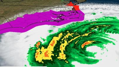
Here we go again. A hurricane is closing in on the U.S. East Coast and General Motors’ OnStar connected car team – now part of something called Global Connected Consumer Experience – is AWOL.

While mandatory evacuations have been ordered and two-way highway connections to the coast have been switched to single direction exit routes to the mainland, OnStar is once again missing an opportunity to offer a public service to its own customers as well as to non-GM-owning drivers. While AAA is posting bulletins and helpful tips for drivers, OnStar remains mute – a glaring lost branding opportunity if there ever was one.

For those unfamiliar with the OnStar connected car platform, OnStar is the more-or-less familiar “blue button” located on the lower rim of rear view mirrors in General Motors vehicles including Chevrolets, Cadillacs, GMCs and Buicks. In fact, GM equips all the vehicles it sells to consumers with this blue button which allows GM vehicle owners to summon emergency assistance in the event of a crash or simply access roadside assistance or other less urgent requests.

Of course, OnStar is most famous for automatically calling for assistance in the event of a cash that results in an airbag deployment – which is especially important in the event of an unconscious driver. All of this means that the OnStar command center in downtown Detroit is receiving requests for assistance along with critical vehicle diagnostic data from cars in and around the hurricane impact zone.

Perhaps more importantly, OnStar is in a position to communicate vital information to its customers in those same zones via its in-vehicle systems or its smartphone apps. In addition, OnStar is in a position to share its view of the entire geographic area correlated to the kinds of requests for assistance that it is receiving – a valuable resource for regional government authorities, news reporting organizations and the general public. But, as a resident of the soon-to-be-impacted area and with a GM owner in my family, I can honestly say GM and its OnStar team are asleep at the switch.

n past hurricanes, such as Katrina among others, GM has turned OnStar on for customers with lapsed accounts and attempted to share evacuation route information. Some day GM will be able to share probe-based traffic information that might help customers and the general public find the clearest routes to safe havens.

But it’s not happening this time. The silence from Detroit is deafening and will soon be drowned out by howling Florence-related winds and the pronouncements from AAA. Where have you gone, OnStar? A nation turns its lonely ears and eyes to you.


Easing Your Way into Portable Stimulus

Easing Your Way into Portable Stimulus
by Bernard Murphy on 09-13-2018 at 7:00 am

The Portable Stimulus Standard (PSS) was officially released at DAC this year. While it will no doubt continue to evolve, for those who were waiting on the sidelines, it is officially safe to start testing the water. In fact it’s probably been pretty safe for a while; vendors have had solutions out for some time and each is happy to share stories on successful customer pilot projects. And I’m told they’re all lined up with the released standard.

That said, PSS obviously isn’t mainstream yet. According to Tom Anderson, who provides marketing consulting to a number of companies and has significant background in this domain, you might think of PSS adoption today as not so different from where formal verification was ~10 years ago – early enthusiasts, pilot projects, likely more innovation and evolution required before it becomes mainstream.

Different people probably have different takes on PSS but for me the motivation isn’t hard to understand. SoC verification engineers have been screaming for years for a way to better automate and accelerate system-level testing while driving better coverage and better reuse of verification components. PSS is what emerged in response to that demand.

Some were upset that PSS wasn’t just an add-on to UVM, but this shouldn’t be too surprising. We’ve already accepted that we need multiple different types of modeling tool – from virtual prototyping to formal verification, software simulation, emulation and FPGA prototyping – because the verification problem is too big to be managed in just one tool. The same applies to verification methodologies – from ad-hoc testbenches to UVM to PSS – because, again, the verification problem is too big to be managed in one verification methodology. UVM is great for the block/IP-level task, but if you’re an architect or a full-system verifier, you’ll probably welcome PSS as a platform much better suited to your needs.

Still, new languages undeniably create new learning curves. For a variety of reasons, PSS comes in two flavors – C++ and Domain-Specific Language (DSL). Demand for C++ unsurprisingly evolved from the software folks. DSL as I understand it is designed to look more familiar to SV users. This split may seem unnecessarily fragmented to some but remember the range of users this has to span. I’m told the standard has been tightly defined so that features in each use-model are constrained to behave in the same way.

PSS adds another wrinkle – it’s declarative, unlike probably most languages you’ve worked with, which are procedural (C, Perl, Python, SV, UVM, …). In a procedural (test) language, you describe how to perform a test; in a declarative language you describe what you want to test and let the tool figure out how. Constrained random does some of this, but still heavily intermixed with details of “how”. Declarative languages such as PSS go further, making test development easier to reuse but also making thinking about test structures a bit more challenging.

So given this, if you want to experiment with PSS, who you gonna call? The simulation vendors of course for compilers / constraint solvers / simulators. They also provide nice graphical tools to view task graphs and generated paths through those graphs. But if history is any indicator, many verification engineers aren’t big fans of graphical creation tools. Most of us prefer our favorite text or “studio”-like editors which may provide additional support for class browsing, autocompletion and similar functions.

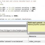
AMIQ recently added support for PSS in the very rich range of design languages they support through their Eclipse-based integrated development environment (IDE). This provides on-the-fly standard compliance checking, autocomplete, intelligent code-formatting, code and project navigation through links, search, class-browsing and integration with all the popular simulators and revision control systems. The figure above shows DVT Eclipse DVE offering an auto-completion suggestion to fix a detected syntax error.

AMIQ supports both C++ and DSL users. Tom tells me that each finds different value in the tool. For the C++ users, the real benefit is in class library support. For DSL users, that the language is close to SV is both a plus and a minus – it’s familiar but also it’s easy to make mistakes. On-the-fly checking helps get around those problems quickly.

Tom wrapped up by acknowledging that in PSS, everyone is learning; there are no experts yet. You can choose to learn quickly in an IDE or you can choose to learn slowly, alternating between your editor window and the LRM. I know, I’m just as bad as everyone else in wanting to stick to my favorite editor, but maybe there’s a better way. You can learn more HERE.

Also Read

CEO Interview: Cristian Amitroaie of AMIQ EDA

Automated Documentation of Space-Borne FPGA Designs

Continuous Integration of RISC-V Testbenches


Fuzzing on Automotive Security

Fuzzing on Automotive Security
by Alex Tan on 09-12-2018 at 12:00 pm

The ECU. That was the service department prognosis on the root cause of thealways-on air bag safety light on my immaculate car. Ten years ago the cost for its replacement with after market part was at par with getting a new iPhone 8. Today, we could get four units for the same price and according to data from several research companies, the ECU market size in 2018 hovers between USD 40 to 63 billion.

ECU (Electronic Control Unit) is central to a vehicle electronic system. The average number of ECUs in today’s medium size car grows to around 40, but could be well over 100 with a highly engineered car as the increased integration of advanced driver assistance systems (ADAS), infotainment, powertrain and chassis electronics are becoming more prevalent. All of these units are interconnected with system buses to perform thousands of vehicle related functions. The move towards more code driven automotive requires complex embedded software and hardware interactions such as sensors driven collision avoidance by brake activation or skid mitigation due to loss of tractions.

Failure, Faults and Fuzzing
As a common means to measure and document the safety level of their systems, ISO 26262 defines requirements for systematic failure and hardware failure verification. The former is related to common design bugs identified with functional verification, while the later involves the use of fault injection to validate certain assumed safety mechanism functionality.

Random hardware failure in automotive domain is a probable event and its impacts could potentially be catastrophic. The process relating to its risk, analysis, remedies and metrics were captured in ISO 26262 functional safety standards among others.

As implied by its name, the triggering origin of such hardware faults could be random and could be external to the subjected system such as an extreme ambient temperature increase due to a mechanical malfunction or an electronic interference. They can however, be modeled based on its inherent characteristics and classified using a formal COI (Cones of Influence). COI helps visualize the potential correlation between the probability of a fault causing a safety critical failure through analyzing six different categories: safe, single-point, residual, detected dual-point, perceived dual-point, latent dual-point.

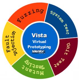
A common form of fault injection method is called fuzzing(fuzz testing), which involves applying anomalous input stimulus to a system to see how it handles it. It is a form of vulnerability analysis and testing derived from the early day of software stress test, some may refer it as the ultimate of black-box approach to security testing. The main benefit of fuzzing includes a minimal up-front effort in capturing the test patterns and optional understanding of DUT (Device Under Test) specifications.
Fuzzing classification is based on the premise of how much prior knowledge assumed on the DUT. A minimal understanding causes more reliance on randomness and mutation based anomalies (a.k.a dumb fuzzing), while having some understanding on the DUT (such as protocol used) leads to fuzzing with generated based anomalies (smart fuzzing). Figure 2 illustrates how fuzzing process on a DUT entails.

Virtual Prototyping and Security
Combining both fuzzing and virtual prototyping delivers many benefits over conventional hardware centric approaches to security testing. Software driven data acquisition and test profiling during debugging steps provide automation and less costly implementation.

Vista Virtual Prototyping is part of Mentor Vista™ platform that provides an early hardware functional model prior to its availability and can run software on embedded processor models at speeds on-par with the actual hardware. It is tightly integrated withSourcery™ CodeBench Virtual Edition to provide additional debug capabilities related to complex software/hardware interactions and the ability to optimize the software to meet final product performance and power goals. Vista has non-intrusive tracing technology and accommodates the use of flexible interfaces to inject various faults and/or packets based on interface protocols. Bypassing physical connection between fuzzing tools and DUT can be done as well in virtual prototyping platform by directly embedding the interfaces models in software.

FFRI, a Tokyo-based computer security firm with global presence demonstrated the use of automated fuzzing coupled with Mentor Vista Virtual Prototyping and FFRI’s Raven testing suite (as fuzzer) to eliminate security vulnerabilities in vehicle ECU under development. As illustrated in Figure 4, the test environment involves a vulnerable software application susceptible to stack-based buffer overflow and monitoring scheme of packet transactions at the guest network interface port to identify the HTTP packet that triggers buffer overflow in the target application.

To simplify the analysis step, a GNU debugger is linked to the system and used as the analysis tool. This enables performing virtual prototyping based testing remotely and automating fuzzing tests in the Vista VP environment through scripting on the host side –allowing a restart should a freeze is encountered.

As a case example, a segmentation fault occurs as a consequence of a stack-buffer overflow event and halts the application –allowing analysis of all frames in the stack. FRRI was able to root cause the segmentation fault through the debugging step, and believes that such approach can be expanded to cover also more complex systems security testing and analysis.
Using this method, a profile can be generated (as shown in Figure 5) and used to identify weak points, thus improving the overall system security robustness against potential side-channel attacks (such as timing or power analysis-based), which may acquire confidential system information.

With the exploding number of code content in modern cars (embedded as part of increased ECU numbers), it is imperative to devise a method to detect safety defects early in the automotive software development process –since deferring fault injection based testing late in the ECU development cycles is costlier. The neat thing about using virtual prototyping coupled with fuzzing allows multi-scenarios testing early and provides cold reboot flexibility.

For more details on Vista check HEREand for FFRI whitepaper check HERE


2018 Semiconductor Winners and Losers

2018 Semiconductor Winners and Losers
by Daniel Nenni on 09-12-2018 at 7:00 am

This is an ongoing conversation inside the semiconductor ecosystem, especially when I am traveling. Everyone wants to know what is going on here or there and since I just returned from Taiwan I will post my thoughts. Last week was also my birthday which was cut short due to the time change but I did get preferential treatment on the flight and at the hotel. Upgrades, champagne, treats, and a full-fledged cake from Hotel Royal in Hsinchu. Either I haven’t traveled on my birthday before or they didn’t roll out the red carpet last time or I would have remembered this, absolutely.

My choice for #1 winner is of course TSMC. They are having a great year and will continue to do so, my opinion. GF ending 7nm put AMD firmly in place at TSMC, Intel is rumored to be moving more products to TSMC, and of course Apple and the rest of the industry has already taped-out to TSMC 7nm so get the marching bands and the dragon dance ready for the end of year celebration.

One note about the Intel move, it is being reported that processors (Coffee Lake) are being moved to TSMC. I find this highly unlikely. Intel 14nm is in no way compatible to any TSMC process so this would be a redesign and why would Intel do that? It is much more likely that mobile chips would be retargeted for TSMC (SoCs, modems, IoT, etc…). Remember, the Intel Silicon Engineering Group is now run by Jim Keller. Jim was at Apple, AMD, and Tesla before Intel so he knows TSMC. Maybe even the next generation FPGAs since Intel is going to be short on 10nm and the ex Altera folks are very TSMC experienced. Or maybe the GPUs since TSMC is very good at GPUs (NVIDIA). There is a forum thread on this you may want to take a look at: Intel 14nm capacity issue.

Broadcom is another winner. Hock Tan keeps changing the rules of the semiconductor game and there is no telling what he will do next but you can bet it will be disruptive. We all scratched our heads when Broadcom acquired Computer Associates for $18.9B in cash. Hock clarified his strategy in the quarterly call:

Speaking of acquisitions, before I turn this call back to Tom to talk about the financials in greater detail, let me perhaps take a few more minutes and talk about CA Technologies. The number one question we get from when we get with CA is, why did we choose to buy? Cut to the chase. We’re buying CA because of the customers and their importance to these customers. CA sales mission critical software to virtually all of the world’s largest enterprises. These are global leaders in key verticals including financial services, telecoms, insurance, healthcare and retail. And CA does it a scale fairly unique to the infrastructure software space. This can only come from longstanding relationships with these customers that spend several decades. In other words, these guys are deeply embedded… https://www.legacy.semiwiki.com/forum/f302/interesting-notes-broadcom-q3-2018-call-10764.html

I also consider GF a winner with their new boutique foundry pivot. I covered this in a previous post GLOBALFOUNDRIES Pivoting away from Bleeding Edge Technologies.

For losers I would start with Intel. 10nm is still in question and even more loserish is the way they disposed of their CEO who spent his entire career at Intel. I cannot believe a Silicon Valley icon like Intel would do such a despicable thing to a 36 year veteran. Clearly it was sleight of hand, waving one hand so you do not see what the other is doing, or not doing in this case. Replacing a questionable CEO with a temp CEO who has publicly declared he does not want to be CEO while you spend months looking for a new CEO? The big question I have is: Why is the Intel Board of Directors NOT being held accountable for this blunder?Correct me if I’m wrong here but this does not pass the corporate smell test.

Let’s continue this discussion in the comments section. Who do you think the semiconductor winners and loser of 2018 will be?


What the world should not learn from Silicon Valley

What the world should not learn from Silicon Valley
by Vivek Wadhwa on 09-11-2018 at 12:00 pm

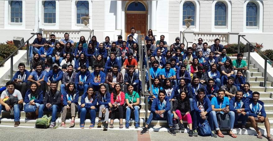
Learn all you can from the entrepreneurs of Silicon Valley but don’t become like them. This was my advice to a group of 91 Indian students who are visiting here on a program sponsored by Rajasthan Chief Minister Vasundhara Raje. In a talk I gave this weekend, I encouraged them to take home the Valley’s optimism and culture of openness and information sharing—but not its greed and obsession with making money.

I also explained the advantage they have over most of the people they are meeting: an understanding the true problems of humanity. This is what gives these students the ability to solve these.

Living here in California, surrounded by beautiful state parks, being close to mountains and the ocean, and having incredible comforts and luxuries, it is easy for entrepreneurs and investors to forget the realities of the world. People here cannot comprehend the hunger, misery, disease, and suffering faced by majority of people on this planet. That is why the vast majority of the billions of dollars that are invested every year by Venture Capitalists go to silly apps and other equally meaningless, mindless projects.

I told the budding entrepreneurs that they have opportunities that their parents could not even have imagined. They can literally build the Star Trek future that we have dreamed about, taking humanity from eons of scarcity to an era of abundance, to a world in which we worry more about sharing prosperity than fighting each other over what little we have. This period in human history is unique, because now entrepreneurs can do what only governments and big companies could do before.

With the advances in computers, which keep getting faster and smaller, the smartphones we carry in our pockets are many times more powerful than the Cray supercomputers of the ‘70s and ‘80s were. Those were only for scientific research and defense—and cost in the tens of millions of dollars. Our phones also have advanced sensors such as accelerometers and gyroscopes, more accurate than those in old nuclear missiles, and cameras with higher resolution than what spy satellites had.

Artificial Intelligence has advanced to the point that it can analyze large amounts of data and help improve decision-making in every sector from agriculture to finance to transportation. The same tools used by engineers at Google and Microsoft—and government research labs—are available to startups everywhere. These can be downloaded for free on the web and mastered by watching YouTube videos.

Robots are already beginning to do the jobs of humans in manufacturing plants, in grocery stores, in pharmacies, driving cars, and making deliveries. The humanoids of science fiction are also becoming a reality. The actuators and sensors necessary to build robots that resemble Rosie from the TV series The Jetsons or C-3PO from Star Wars are commonly available and inexpensive. AI will soon take a few more leaps forward and provide these the capability of acting intelligently—just like what we imagined.

There is no reason that Rosie can’t originate from anywhere in the world—and speak Hindi or Mandarin.Using CRISPR, a new gene-editing system derived from bacteria that enables scientists to edit the DNA of living organisms, it is becoming possible to eradicate hereditary diseases, revive extinct species such as the woolly mammoth, and design plants that are far more nutritious, hardy and delicious than what we have now. Imagine banana and mango plants that thrive in the desert of Rajasthan. These may, one day, be a reality. This is all terrifying and amazing at the same time and relatively inexpensive to do by anyone, anywhere, using the tools.

These are just a few examples of what new technologies are enabling. In the next decade, we will also be 3D printing household goods, entire buildings, electronic circuits, and even our food. We will be designing new organisms that improve agriculture and clean up the environment. We will be delivering our goods—and perhaps be transporting ourselves—by drone. We can also build futuristic cities, which use only renewable energies, are clean and self-sustaining, and provide incredible comforts.

Amazing and good things really are possible. Yet, the same technologies can create dystopia, with large-scale destruction, spying, pandemics, and other unimaginable horrors. Many social and ethical dilemmas lie ahead.

You can be sure that governments and investors are funding the most profitable and malicious uses of technologies. That is why it is so important to teach the world’s entrepreneurs about the advances and to inspire, motivate, and support their efforts. They will surely put technologies to their best uses and do this out of concern for humanity rather than just a profit motive.

For more, read my book, The Driver in the Driverless Car,and follow me on Twitter: @wadhwa


DesignWare IP as AI Building Blocks

DesignWare IP as AI Building Blocks
by Alex Tan on 09-11-2018 at 7:00 am

AI is disruptive and transformative to many status quos. Its manifestation can be increasingly seen in many business transactions and various aspects of our lives. While machine learning (ML) and deep learning (DL) have acted as its catalysts on the software side, GPU and now ML/DL accelerators are spawning across the hardware space to provide performance leaps and growing capacity to the compute hungry AI data processing needs.

For the past few decades EDA has bridged the hardware and software space, transforming many electronic design challenges into solutions that became key enablers or drivers for its adopters to push the technology envelopes further. Being at the HW and SW technology crossroad, many EDA providers have embraced AI by either having their solutions augmented with ML assisted analytics or expanding its features to enable AI centric designs or applications.

AI Enablers and Challenges
According to nVidia CEO Jen-Hsen Huang, the rise of AI had been enabled by two concurrent disrupting dynamics, i.e., how software development is done by means of deep learning and how computing is done through the more adoption of GPU as replacement to single-threaded, multi-core CPU, which is no longer scale nor satisfy the current increased computing needs.

Let’s consider these two factors further. First, the emergence of more complex DL algorithmic models such as CNN (convolutional neural network) and RNN (recurrent neural networks) has made AI based pattern recognition applications such as embedded vision and speech processings more pervasive.
Training and inferencing steps, the two inherent and needed ML traits which mimic human cognitive development aspects, are subjected to different challenges. The former requires sufficient capacity and bandwidth, while the later demands latency optimization as it deals with irregular memory access issue.


Secondly, on the hardware side, a CPU typically has a few to several dozens of processing units, some shared caches and control units. CPU is multi-purpose but has limited capacity. In contrast, a GPU employs numerous (hundreds to thousands) processing units with their own caches and control units, which are dedicated to perform specific works in parallel. This massive array of compute power and parallelism can absorb the workload presented by deep learning applications. GPU is well suited for training steps as it requires floating point engine while the inferencing portion may resort on a reduced accuracy or integer based data processor. Challenges to GPU architecture include the availability of adequate interconnect speed and bandwidth.

Aside from the above two factors, the advent of FinFET process technology has also played a major role in accommodating the integrations of the billions of devices into foundry allowed silicon die active area.

SoC and DesignWare Building Blocks for AI
Synopsys DesignWare® IP portfolio has been the foundation to chip design implementation for over two decades, containing technology- independent design IP solutions optimized for various cost factors (PPA). As DesignWare is at the epicenter of the ever evolving SoC implementation space, the list of DesignWare building block IP solutions has grown over the years, from a few number of compute primitives such as adders, multipliers to increasingly complex IP blocks such as microcontrollers, interface protocols (AMBA, USB, etc.) and eventually embedded microprocessors, interconnects and memories. Its integration also has been expanded to not only cover synthesis integration but also facilitate virtual prototyping and verification IP.

Designing SoCs targeted for AI related applications requires specialized processing, memory performance and real-time data connectivity. Recently, Synopsys upgraded its DesignWare IP portfolio for AI to also include these DL building blocks.

Specialized Processing
Specialized processors include embedded processors and tools for scalar, vector, and neural network processing. In order to handle AI algorithm efficiently, machine vision has relied on a heterogeneous pipelined processing with varying degree of data-centric parallelism.

As illustrated in figure 3, there are four stages associated with a visual data processing. The pre-processing step has the simplest data parallelism while the precise processing step has the most complex, requiring good matrix multiplication capabilities. Such unique processing needs can be served by Synopsys DesignWare ARC® processors. The DesignWare ARC EV6x processors integrate a high-performance scalar RISC core, a vector DSP, and a convolutional neural network (CNN) engine optimized for deep learning in embedded vision applications. The ARC HS4xD and EMxD processor families combine RISC and DSP processing capabilities to deliver an optimal PPA balance for AI applications.

Memory Performance
AI models demand large memory footprint contributing to the overall silicon overhead as training neural networks requires massive memory space. Synopsys’ memory IP solutions include efficient architectures for different AI memory constraints such as bandwidth, capacity and cache coherency. The DesignWare DDR IP addresses capacity needed for data center AI SoCs.

Furthermore, despite the sustained accuracy promised by AI model compression through the pruning and quantification techniques, their adoption introduces irregular memory access and compute intensity peaks –both of which degrade the overall execution and system latency. This also drives the need for more heterogeneous memory architectures. DesignWare CCIX IP enables cache coherency with virtualized memory capabilities for AI heterogeneous compute and reduces latency in AI applications.

It is common that parallel matrix multiplication and increased size of DL models or coefficients necessitate the use of external memories and high bandwidth accesses. The DesignWare HBM2 IP addresses the bandwidth bottleneck while providing an optimized off-chip picojoules (pJ) per bit memory access. A comprehensive list of embedded memory compilers enabled for high density, low leakage, and high performance on-chip SRAMs options as well as TCAM and multi-port flavor are also available. Most of them are also ported to 7nm FinFET process node.

SoC Interfaces and Real-Time Data Connectivity
Synopsys also provides reliable interface IP solutions needed between sensors. For example, real-time data connectivity between embedded imaging vision sensors and deep learning accelerator engine, normally done at the edge, is crucial as it is power sensitive. Synopsys offers a broad portfolio of high speed interface controllers and PHYs including HBM, HDMI, PCI Express, USB, MIPI, Ethernet, and SerDes to transfer data at high speeds, with minimal power and area.

Although DL SoCs have to deal with fluctuating energy metrics per operation due to massive data movement on and off chips, having both power management supported by memory IPs and the adoption of advanced FinFET process nodes such as 7nm, could provide an overall effective power handling.

As takeaways, designing for AI applications requires the understanding of not only the software or application intents but also the underlying data handling in order to deliver an accurate prediction within a reasonable compute time and resources. Having Synopsys’ silicon-proven DesignWare IP solutions as the building blocks will help accelerate the design realization while providing design teams with opportunities to explore an optimal fit to the more heterogeneous design architecture.

For more info on Synopsys DesignWare IPs please check HERE .


Affordable EDA Tools for IoT Designs, Guess which Vendor

Affordable EDA Tools for IoT Designs, Guess which Vendor
by Daniel Payne on 09-10-2018 at 12:00 pm

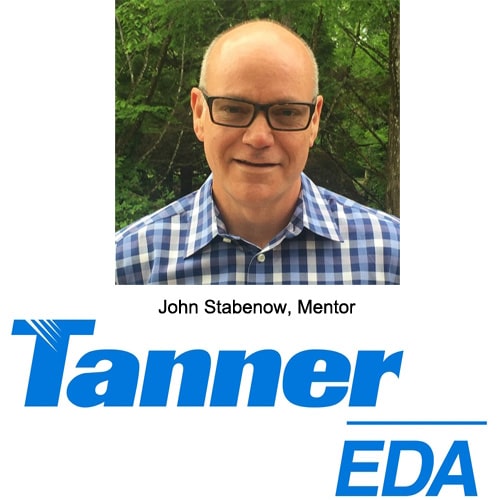
I just had to drive my car 7 miles from Tualatin, Oregon to visit with an EDA veteran who has played a lot of diverse roles in his career, including: IC Mask Designer, Layout Manager, Account Manager, Business Development, Director, Foundry Relations Director. His name is John Stabenow, with Mentor, a Siemens Business, and we met in Wilsonville, Oregon last month to talk about Tanner EDA. I’ve known John for awhile and he’s worked with all three major EDA vendors over the years, so has a really deep perspective especially on the IC side.

Q&A

Q: What is the sweet spot for companies using Tanner EDA tools these days?

Our IC design customers are using 28nm and above nodes, often building diverse IoT systems that may even use MEMS, RF and require AMS IP.

Q: Can you name a trend among Tanner EDA customers doing IoT designs?

Sure, in the past there were separate companies doing sensor design and chip design, but now we see these sensor component companies branching out into doing their own chip designs that connect to the sensors. The IoT is really about sensor-driven design, and IoT edge systems are using lots of sensors.

Q: How about getting started with an IoT that uses a processor core?

We’ve partnered with ARM so that you can do a core-based design concept using an ARM M0 or M3 at no cost, in order to get your project started. It’s part of the ARM DesignStart program and we started this back in 2016.

Q: I mostly think about Tanner EDA as full-custom IC tools, so how do you get digital tools like P&R or synthesis?

Mentor has a lot of digital implementation technology, so we make available a version of Nitro for P&R and Oasys-RTL for synthesis to Tanner EDA users. For smaller designs you can choose to use the Tanner EDA Place and Route tool within the Tanner L-Edit tool.

Q: Are Tanner tools only available on the Windows platform?

Historically the Tanner EDA tools were first offered on the Windows platform, then we’ve expanded that to include Linux using the Wine technology. On a side note, 2018 marks Tanner’s 30th anniversary, which I think makes Tanner a little older than Virtuoso.

Q: Where do I get a PDK when using Tanner tools?

We have a PDK team at Tanner where they create, QA and migrate all of the kits, collaborating with the foundries to create iPDKs.

Q: Any new tools coming out of Tanner recently?

You bet, there’s Tanner Designer, it’s a tool for analog verification management where you can track all of your tests in one place and determine how complete your testing plan is. The tools uses an Excel interface, so it’s intuitive to learn and setup, supporting simulators like: T-Spice, Eldo and AFS.

Q: Mentor has a lot of SPICE circuit simulators, so what do you recommend for Tanner users?

It depends a little on the customer. For some of our customers, we suggest that for day to day usage give T-Spice a try, then at sign-off you can switch to either Eldo or AFS simulators. IoT designers doing RF circuits will want to work with Eldo RF. Our enterprise customers are asking for Eldo or AFS, so we have integrations to both.

Q: Can I do photonic chip designs with Tanner tools?

Yes, you take a combination of the L-Edit tool and Luceda IPKISS.eda to enable photonic IC layout design for things like an Arrayed Waveguide Grating (AWG) with our Filter Toolbox, and also use our library of photonic components. We also have a strong partnership and mutual customers with Lumerical.

Q: What should I expect in future releases of Tanner tools?

You will see layout productivity improvements that will include layout generators, stay tuned.

Q: I know that Mentor acquired Tanner EDA, but now Mentor was acquired by Siemens, so how’s that all going?

The Siemens acquisition of Mentor has been one of the smoothest transitions ever, we still have our Tanner identity and are in growth mode for our product revenue and number of customers. Tanner EDA is bringing new customers into Siemens that they have never seen before. About 35-40% of new Tanner customers are new to Mentor. This acquisition by Siemens has been good for Tanner EDA.

Q: SoftMEMS was a partner of Tanner EDA, so how is that relationship doing?

Tanner EDA and SoftMEMS are still active and collaborating quite well in the field. There’s an on-demand webinarthat shows you more about the technology.

In the MEMS area we’re winning new customers, even beating Coventor tools.

Related Blogs


The Rebirth of Dolphin Integration!

The Rebirth of Dolphin Integration!
by Eric Esteve on 09-10-2018 at 7:00 am

You may have seen this Press Release (see below) announcing that Dolphin Integration (Dolphin) has been acquired by Soitec (60%) and MBDA (40%) – you can see more information about these two companies at the bottom of this blog. Founded in 1985, Dolphin had some recurrent cash flow issues during the last couple of years, that they solved by using bank loans. Even if the company was doing profitable business, the bottom line was negative.

Like it frequently happen in the US when a company goes to Chapter 11, Dolphin Integration management initiated in June an insolvency recovery process. Dolphin is one of my customers, I know their IP port-folio and also their new CEO since February, Christian Dupont, that’s why I want to share my personal opinion about the company.

This acquisition is an opportunity, a great opportunity for Dolphin to deploy their Energy efficient IP based new strategy and satisfy their European customers in the Defense/Aeronautic industry by delivering top class ASIC design & supply services. Let’s concentrate on their impressive IP port-folio: Dolphin has developed 600 IP (mostly mixed-signal) for about 500 customers WW! These IP can be ranked in three categories: Foundation, Features and Power Management IP.

Thefoundation IP, libraries and memory compilers, optimized for the best trade-off between power consumption and area support major Silicon foundries, all the way down to 22nm. Such foundation IP are even available foundry sponsored in major node, and Dolphin development team has a very good reputation. In fact, there is no other option than targeting the highest quality level when you deliver this type of IP to a foundry, as their customers will use it to design their SoC. No doubt that this business will expand if you consider the multiple process variants built around a single process node, and the diverse technology options, bulk or FD-SOI.

By Features IP, Dolphin consider an IP family, mostly built to support audio chip, where mixed-signal design expertize is key. Thanks to 30+ years experience of the company in this field, requiring an unique understanding of application-related audio challenges, they can do better and faster than new-comers, leading to better differentiation and faster TTM for their customers.

The Power Management IP family deserve an explanation: we talk about all these functions that you have to use to efficiently design energy optimized IC. To my opinion, this family has a huge growth potential as it target most application and is critical for the battery powered SoC. Decreasing the power consumption is becoming the next goal, like offering always higher frequency in the 2000’s. In fact we should say making better power efficiency, it’s more accurate.

In the Moore’s law golden age, a chipmaker had just to re-design to the next technology node to automatically benefit from higher performance and lower power consumption-at the same time! This is still true, but only for those who can afford to move from 10nm to 7nm, and this is not the majority. The others will have to be smarter, integrating Dolphin’s Power Management IP is a way to design more power-efficient SoC. This is true for IoT edge SoC and for battery-powered chip in general, and this is also true for automotive advanced application, where power consumption is a real concern.

By the way, Dolphin has already more than 10 customers in this automotive segment, and there is no doubt that they will quickly develop this customer base. The company is European based, which will certainly help.

Let’s mention this quote, from E. Lozano, Sr. Director of Business Development and IP Solutions with Open Silicon: “Dolphin Integration is a leading silicon IP provider for low power IoT SoCs. In view of the growing demand for low power consumption in IoT devices, we intend to leverage the unique solutions offered by Dolphin Integration to meet the challenges of our IoT customers.”

From an organization standpoint, Dolphin will operates independently from Soitec and MBDA, while obviously benefiting from each company ecosystem. But that doesn’t means that Dolphin will limit to FD-SOI based SoCs! It would be a mistake to do so… They are and will stay multifoundry and they will follow their customers in term of process or CPU choice.

In term of positioning, Dolphin will have the opportunity to focus the marcom resource where it’s needed the most to sell on a WW market, the IP products. The group in charge of ASIC design services will satisfy existing customers in Europe, but has not the charter to develop a WW business.

In fact, the Dolphin’s strategy is simply to be the best “Energy Efficient IP Company”. If you look at their port-folio, that makes sense at 100%: Power Management IP are allowing to architect SoC for better power efficiency. This will be well complemented by their feature IP like Audio IP (frequently integrated into battery-powered IC), and power-optimized libraries or memories. Power efficiency is becoming as important as pure performance, as you can see with this extract from a PR from Huawei (August 2018) about the Kirin 980:

“Debuting with the Kirin 980, Mali-G76 offers 46 percent greater graphics processing power at 178 percent improved power efficiency over the previous generation.”

Despite this summer insolvency recovery process, Dolphin acquisition by Soitec and MBDA is a real opportunity for the company to rebound and focus on what they do best, efficient IP development. Their positioning on power efficiency IP targeting battery-powered SoC as well as automotive and probably infrastructure application (which suffer from power dissipation limitation) is well aligned with the next decade strong market trend to develop power efficient SoC (in my opinion).

To see the PR, use thisNasdaq link

ByEric Esteve fromIPnest

About Soitec
Soitec (Euronext, Tech 40 Paris) is a world leader in designing and manufacturing innovative semiconductor materials. The company uses its unique technologies and semiconductor expertise to serve the electronics markets. With more than 3,000 patents worldwide, Soitec’s strategy is based on disruptive innovation to answer its customers’ needs for high performance, energy efficiency and cost competitiveness. Soitec has manufacturing facilities, R&D centers and offices in Europe, the U.S. and Asia.

Soitec and Smart Cut are registered trademarks of Soitec.
For more information, please visitwww.soitec.com and follow us on Twitter: @Soitec_EN

About MBDA
MBDA is the only European group capable of designing and producing missiles and missile systems that correspond to the full range of current and future operational needs of the three armed forces (land, sea and air).

With a significant presence in five European countries and within the USA, in 2017 MBDA achieved revenue of 3.1 billion euros with an order book of 16.8 billion euros. With more than 90 armed forces customers in the world, MBDA is a world leader in missiles and missile systems. In total, the group offers a range of 45 missile systems and countermeasures products already in operational service and more than 15 others currently in development.
MBDA is jointly owned by Airbus (37.5%), BAE Systems (37.5%), and Leonardo (25%).
For more information, please visitwww.mbda-systems.com



Is the Q4 Bounce Back now a 2009 Recovery?

Is the Q4 Bounce Back now a 2009 Recovery?
by Robert Maire on 09-10-2018 at 7:00 am

Last week saw a unique confluence of events that continue the negative news flow in semicap following the story about GloFo. At a financial conference, Micron’s CFO said NAND prices were declining, this was on top of an analyst note in the morning about the same issue. Even though this should be no surprise as memory has had an overly long strong run.

Then KLAC’s CFO tempered expectations for the balance of the year due to the pushout of DRAM business that was already announced and well known in the industry. (Samsungs pushout of spending..)

Also read: GLOBALFOUNDRIES Pivoting away from Bleeding Edge Technologies

Separately either topic is well known and out in the public domain already but being “announced” at the same time in the first conference back from the summer sets an ominous tone, and acts like a catalyst.

Micron announcing declining NAND prices is like pouring gasoline on the already dry tinder of memory concerns then ignited by a cigarette flicked out the window by KLAC’s comments.

We now have a meltdown…..even though its not a lot of new news and things we have been talking about for a long time….

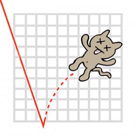
Dead Cat Bounce Done?
Concerns about memory seem to have faded over the summer during vacations when the market is usually quiet but the issue never really went away. We have been very clear that the memory run was too strong for too long and well overdue for a correction that we had already started to see months ago.

Falling NAND pricing or DRAM pricing should be no surprise but perhaps having multiple comments on the first day back are a bit too much…..

Stock had recovered a bit while investors took their eye off memory concerns and we had a little bit of a dead cat bounce but now it sounds like multiple doctors are declaring the cat truly dead…….

Q4 “Snapback ” not so “Snappy” now
While the vast majority of analysts and bulls on the stocks rushed out in support of a one quarter downturn, we took a more conservative view suggesting we were very “dubious” as it would make absolutely no sense for Samsung to push out only one quarter. It now seems our more conservative view may be borne out as we are now talking about 1H19 recovery (maybe…). While CQ3 may still be the “trough”, but the length of the trough and the angle of recovery out of the trough is more questionable.

GloFo not that impactful..

The reality of last weeks news about GloFo dropping out of the 7NM race while surprising is not hugely impactful on the revenues of semicap companies. The reality is that most tool makers had long ago discounted GloFo as a major player and discounted the revenue expectations from them. The real issue is more the view that it is additional negative news and the ability to make up for a memory shortfall from the foundry side all that much more difficult.
So while the GloFo news itself is not that negative, its when its taken in context with the overall negative news flow we are experiencing.

KLAC bulletproof vest weakened
KLAC’s “defensive” play ,which up until now has been working, is obviously taking a bit of a hit. KLAC’s stock which has held up way better than AMAT & LRCX due to its lower memory exposure is now leading the group lower today. This lower memory exposure premium the stock has enjoyed will obviously be reduced now that the same memory issue is impacting KLAC’s financial performance.

To be clear, KLAC still has much less memory impact than AMAT or LRCX, but it does not have zero impact. The foundry side of KLAC’s business is unaffected and still very strong.

The stocks
Today is an ugly wake up call after a relatively quiet semiconductor summer. There is not a lot of new news here but putting it all together in one place and time is obviously overwhelming the stocks.

We have been very clear, for a long time, that memory was too strong for too long, and had to cool off. Wether it cools slowly or takes polar bear plunge matters little. It actually may have been better for memory to drop quickly and get it over with rather than reliving the fear of memory pricing dropping over and over again.

Likewise with the semicap stocks, its time to get over the fact that the industry is still cyclical and goes up and down. Customer concentration is making that worse. It is also naive to assume only a one quarter, or one company, slow down. All the cyclical downturns we have seen have more than one negative issue.

We had said that AMAT had downside to the low $40’s and we are there. We had also said that LRCX could have downside to $150ish but we are still a bit above that. KLAC may have lost about a 10% premium that it has held as a “defensive” play.

Micron is very, very cheap and getting cheaper. The negative memory discount has been applied too many times as the company is still making a lot of money.

We probably have another 6 weeks or more until companies report and we get a sigh of relief as fears turn into reality which is usually less negative than the anticipation itself.

In the meantime we find it hard to catch a falling spear and buy into this continuing flow of negative news especially given the skittishness of the overall market.


Mentor Graphics Makes a Transition

Mentor Graphics Makes a Transition
by Daniel Nenni on 09-07-2018 at 12:00 pm

This is the fourteenth in the series of “20 Questions with Wally Rhines”

I joined Mentor Graphics (now Mentor, A Siemens Business), in late 1993. Tom Engibous, one of my direct reporting people at TI, was promoted to replace me as head of the Semiconductor business of TI and I moved on to what I knew would be a real challenge, the rescue of an EDA company that had committed to a strategy that was likely to fail; I knew all this because I was a large customer for Mentor at TI. But my wife thought that Portland would be a good place to raise our very young children and Jerry Junkins, the CEO of TI, made it clear to me that any succession to his role wouldn’t happen for at least ten years because of his own career plans.

I came to Mentor with an optimistic view. After all, most companies that have failed product generations can quickly shift to other innovations they have on the shelf and re-generate their momentum. Not so with Mentor’s Version 8.0 Falcon (later referred to as Version Late dot Slow). There wasn’t a lot on the shelves to build upon and almost everyone in the company had been moved to the Falcon project to try to save it. But the shelves were not totally bare.

My first interest at Mentor was emulation. After all, I knew that Mentor had the best emulation technology in the industry, having visited there to observe it before. When I arrived at Mentor and asked about it, everyone started checking his shoe polish. Unfortunately, Mentor had sold its leading emulation technology, along with the patents, to QUICKTURN, leaving only a very limited ability to compete.

I then turned to physical verification. After all, I had signed the contracts for Mentor to OEM TI’s physical verification software while I was at TI, and it had been a reasonable recovery from Mentor’s loss of Dracula (their OEM solution) when Cadence acquired ECAD and terminated Mentor’s OEM agreement. TI was not interested in extending the OEM arrangement with Mentor to the next generation so we bought out their rights and in January 1994, we had a big kickoff meeting to develop the next generation of physical verification, headed by Laurence Grodd for the physical verification and Koby Kresh for the Logic to Schematic verification. In addition to the fact that Laurence was brilliant, we had the benefit that he had maintained a database of designs that were verified using “Checkmate”, the Mentor name for the product we OEM’d from TI. Laurence could handle hundreds of variants in design style. He proceeded to innovate innumerable approaches to physical verification including selective promotion and other things that are routine today; unfortunately, Mentor didn’t file any patents. So ISS, a company in North Carolina that was ultimately acquired by AVANTI, adopted many of these approaches, including hierarchical forms of analysis.

Internal politics were also a factor, as they always are in large companies. Mentor’s custom IC layout product, IC Station, was in a battle to beat Cadence’s product, Virtuoso. Our physical verification capability in IC Station came from Laurence, was called “IC Verify”, and was clearly superior to competition. So why would we sell it stand-alone to competitors using Virtuoso? Subsequently, a copy of “Calibre” was sneaked out to AMD and their designers became excited by it. Meanwhile, Mentor’s products that had evolved from the TI OEM continued to evolve and Intel became a major customer. The war had begun. At the next DAC, a decision was made to display the new “Calibre” capability and that was a decisive move, undercutting the roadmap that Intel was expecting. While the Intel surprise was upsetting for some in our sales force, Calibre clearly ushered in a whole new generation of physical verification.

The critical role at this time came to Brian Derrick, GM of the Physical Verification Division. Brian did something very innovative, and probably forbidden in most large companies. Brian worked directly with Danny Perng, a salesman in Taiwan who was interested in focusing on Calibre for the foundries, TSMC and UMC. Because our sales force knew that TSMC and UMC wouldn’t pay much for tools, the sales and support resources in Taiwan were insufficient to drive a foundry campaign. So without permission, Brian hired his own sales force to complement Danny’s effort. These specialists from the product division were able to convince the TSMC engineers, and later those at UMC, GLOBALFOUNDRIES, etc., that Calibre was superior to competitive approaches.

Simultaneously, Brian’s team concluded that optical proximity correction would be the next important extension of physical verification. Presim, a startup based in Portland, Oegon, was the leader and they had captured the Intel account. Not to be defeated, Brian found the leading experts in the technology (going to UC. Berkeley to find OPC Technology Inc. and hiring Nick Cobb to head up the development). These strategic moves created the basis for Mentor’s #1 position today in both physical verification and resolution enhancement.

Of course there were many more battles to win (and lots of fun yet to be experienced). Whenever I ask successful people in technology, including CEO’s, about the most enjoyable part of their careers, they almost always point to a period when they worked with a group that overcame the impossible and developed a product or capability that changed an industry. Calibre provided just such an experience for many, as did a number of other developments that emerged on Mentor’s path to recovery.

Mentor had undergone lots of problems and had moved from #1 to #3 in a competitive EDA industry. It was clear that we had found areas where we could be the defacto standard: Calibre physical verification, Tessent Design for Test, Expedition PCB Design, Calypto/Catapult high Level Synthesis, Automotive Embedded Electronics, and eight others by the metric provided in the official Gary Smith EDA analyses. Fortunately, Synopsys eventually decided that they didn’t have to do everything; they could pursue new areas that Mentor was not pursuing. That allowed a level of diversification that had not been common in the EDA industry.

And, with that, the EDA industry started to change. Each major EDA company developed specialties, instead of spending all their time trying to take market share from each other. And they all became more innovative. If I could claim one contribution to the EDA industry, it would be this. We are now an industry that looks for capabilities that will help our customers, and then develops (or acquires) those capabilities, rather than just trying to take market share from each other.

The 20 Questions with Wally Rhines Series