webinar banner AI 2026 v2

Improving Yield and Reliability with In-Chip Monitoring, there’s an IP for that

Improving Yield and Reliability with In-Chip Monitoring, there’s an IP for that
by Daniel Payne on 08-24-2018 at 12:00 pm

There’s an old maxim that you can only improve what you measure, so quality experts have been talking about this concept for decades and our semiconductor industry has been the recipient of such practices to such an extent that we can now buy consumer products that include chips with over 5 billion transistors in them. You’ve probably heard that semiconductor IP vendors can offer you an incredible array of choices: Standard Cells, Memory, Processors, Interconnect, Serial IO, PLL, radios, FPGA, converters, and the list goes on. Lesser known are the specialty IP vendors that have deep analog expertise, and one of them is Moortec Semiconductor. Developers at Moortec have specialists that created three classes of in-chip monitoring blocks for:

  • Process Monitoring
  • Voltage Monitoring
  • Temperature Sensing

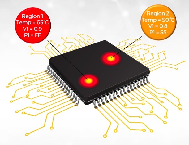
Consider the challenge of reaching timing closure on your SoC where two regions of the same chip have different junction temperatures, VDD supply levels and even process corners:

If your design used in-chip monitoring of Temperature and Process, then you could measure the effects and make system-level decisions to mitigate the effects, per design. Let’s peek a bit deeper into the specific IP that Moortec offers to monitor Process, Voltage and Temperature:

Your chip typically will include multiple sensors at strategic locations in order to measure and control for greatest impact.

Temperature Sensors
The temperature sensor has some impressive specifications that help you know what the junction temperature is across a chip and then take steps to control it:

  • Accuracy of +/- 3C without calibration, +/- 1C when calibrated
  • Resolution of 0.06C
  • An analog test bus for characterization and debug
  • Interface with APB or an I2C
  • Self-checking
  • Different modes for faster sampling: 12-bit, 10-bit or 8-bit

Voltage Monitors
These monitors provide voltage insight for IR drop, core supply, IO supply, and AVS (Adaptive Voltage Scaling). A voltage monitor finds supply events, perturbations and transients. Specifications are:

  • +/- 1% or +/- 0.6% accuracy
  • +/- 1mV accuracy on IR drop analysis
  • Up to 9 channels for 28nm nodes
  • Up to 16 channels for FinFET nodes

Process Monitors
Local variation across an SoC means that there can me multiple process corners present, per die, so being able to measure the process corner is an essential step. The basic circuit for a process monitor is the ring oscillator, so each process monitor contains multiple delay chains to determine which process corner is dominant. The four application areas for a process monitor include:

  • Speed binning during characterization
  • Age monitoring
  • Critical voltage and timing analysis
  • AVS

PVT Controller
The blue area shown above is the PVT Controller and your chip only needs one controller which is then connected to multiple PVT instances. Consulting with Moortec you can best understand how many of each instance your specific chip should have, and where to place these IP cells.

Specifications for the PVT Controller are:

  • Control multiple instances of the Process, Voltage and Temperature monitors across the chip
  • Temperature & Voltage alarms
  • Analytics – max, min, sample values
  • iJTAG access support

The PVT Controller along with monitors enables your engineers to implement:

  • DVFS (Dynamic Voltage Frequency Scaling)
  • Clock speed optimization
  • Power optimization
  • Silicon characterization
  • Improve reliability and device lifetime

Foundry Support
The Moortec Embedded In-Chip monitoring Subsystem is available on various foundries and supports advanced node CMOS technologies on 40nm, 28nm, 16nm, 12nm & 7nm.

Contacts
The team at Moortec has built up world-wide distribution partners, showing just how successful their in-chip monitoring IP has become:

  • UK (Moortec)
  • UK, Europe (AQT)
  • Europe (Sythra)
  • USA (Mark Davitt, Manzanita Semiconductor)
  • Israel (Amos Technologies Ltd.)
  • China (OnePass)
  • Taiwan (Kaviaz)
  • South Korea (Chipinside)
  • Japan (Spinnaker Systems)
  • Russia (Nautech)

Related Blogs


Semiconductors Become a Worldwide Business

Semiconductors Become a Worldwide Business
by Daniel Nenni on 08-24-2018 at 7:00 am

This is the twelfth in the series of “20 Questions with Wally Rhines”

Among the companies that bought a license from AT&T to produce the transistor was Sony. While the U.S. maintained its lead in technology, other countries like Japan emerged as competitors. Semiconductor manufacturing was both labor intensive and capital intensive. Fairchild became the first major semiconductor manufacturer to start operations overseas, adding an assembly site in Hong Kong in 1964 where labor costs would be lower. TI and Motorola followed, although TI began with a misstep by starting an assembly site in Curacao. TI made up for this slow start through a different path – an attempt to sell in the Japan market. After World War II, U.S. companies were not allowed to set up wholly owned subsidiaries in Japan; they had to partner with a Japanese company who would have majority ownership. Companies like IBM and Kodak that had operations in Japan before WWII were grandfathered and could continue with their 100% owned subsidiaries in Japan.

TI wasn’t interested in a joint venture. And Pat Haggerty saw the potential that Japan offered as a future manufacturing power house. So this became the first case of TI using its U.S. patent portfolio for reasons other than defense. The negotiations resulted in permission from the Japan government allowing TI to set up a joint venture with Sony in 1964 merely for appearances. I’m told that Sony people never showed up and TI quietly bought out their share of the business later. But Haggerty established a personal relationship with Morita, founder and CEO of Sony that lasted through Haggerty’s lifetime. This became important in the future.

TI began a successful offshore assembly operation in Hatogaya, Japan on the outskirts of Tokyo, followed by another assembly site in Hiji Japan on the island of Kyushu. The Hiji site was on the top of a small mountain overlooking the ocean on three sides and must have been one of the most valuable pieces of industrial real estate outside Tokyo. This habit of finding valuable real estate for plants was a TI characteristic, rumored to be the responsibility of Board member Buddy Harris. The choice of the TI Nice plant was terrible from the point of view of location for manufacturing but it was on the top of a hill with a panoramic view of the French Riviera. Whatever limitations the site had were, at least partially, offset by the breathtaking view.

Soon the race for offshore manufacturing sites was on. Morris Chang’s influence came to bear and Taiwan would have been the next site but Morris tells me that the Taiwanese government wasn’t flexible enough. TI therefore built the Singapore site in 1968, then Taiwan in 1969, Malaysia in 1972 (simultaneously with Motorola and SGS Thomson in Kuala Lumpur) and the Philippines in 1979 (a site that I was proud to have report to me from 1987 through 1993).

TI did two things that were unique among semiconductor companies in the race to build up offshore manufacturing. First, TI decided that cheap labor was not the only reason to go offshore. The offshore sites had skilled technicians as well. So TI moved automated manufacturing equipment to its offshore sites even though manual labor was cheap. This turned out to be highly advantageous. The other thing TI did was to establish wafer fab manufacturing in Asia, starting in Japan. Intel remained largely in the U.S. Motorola was primarily the U.S. and Europe as were most other semiconductor companies. Europe was necessary, at least for assembly, because they had substantial duties on imported semiconductors. European assembly sites saved money despite the high labor cost. TI, of course, had wafer fabs all over Europe, starting in the UK, then Germany, France and Italy. Assembly sites were limited to Portugal and Italy.

One result of the establishment of wafer fabs in Japan was a creation of awareness of the superb manufacturing process variability control that was possible with Japanese workers. In cases where we sent the same photomask set to Japan, the die sort yields were typically much higher than those of the same devices produced in the U.S. TI used this to its advantage.

When the trade wars between Japan and U.S. semiconductor companies erupted in the 1980’s, MITI (the Japan Ministry of International Trade and Industry) assigned Japanese companies quotas for purchase of semiconductors from U.S. companies. Sony was assigned a very high quota of 20%. All the Japanese companies wanted to fill their quotas with DRAMs but only TI and Micron were still in the business in the U.S. At this time, I was managing an organization I named Application Specific Products, or ASP, that had responsibility for microprocessors and ASICs. Yukio Sakamoto and I went to Japan to negotiate a deal with Sony with a goal of having TI manufacture the chips used in the industry standard Sony Walkman.

Because of the historic relationship between TI and Sony, my meeting started with Norio Oga, the CEO and former opera singer who succeeded Morita as Sony CEO. Sony’s offer: If you can match the Sony Semiconductor internal transfer price and quality, you can have 100% of the business. When we started production, our packaging cost alone for an 84 pin Quad Flat Pack was six cents per pin, more than the total price of the chip plus package. Within four months, thanks to Sakamoto, we were at one yen per pin. Similar ratios existed for the chip. And over the next year, we billed Sony for $200 million for Walkman chips and greatly enhanced our manufacturing capability.

The 20 Questions with Wally Rhines Series


Verifying ESD Fixes Faster with Incremental Analysis

Verifying ESD Fixes Faster with Incremental Analysis
by Tom Simon on 08-23-2018 at 12:00 pm

The author of this article, Dündar Dumlugöl, is CEO of Magwel. He has 25 years of experience in EDA managing the development of leading products used for circuit simulation and high-level system design.

Every designer knows how tedious it can be to shuttle back and forth between their layout tool and analysis tools. Every time an error or rule violation is found, you need to open up the design in the editor and make changes, save, export and re-run the analysis. This is especially true with ESD tools, which are fine for analysis, but often leave designers running blind when it comes to resolving errors. As a result, designers have no recourse other than to iterate back to layout to fix issues. Magwel’s ESDi offers refreshing features for locating the source of an error and, even more importantly, for making changes and testing fixes without leaving the ESD tool itself.

Magwel’s EDSi offers comprehensive and high speed ESD simulation on every pad pair. It takes into consideration competitive triggering so that it more accurately evaluates voltages and currents during discharge events. It also uses I/V curves that can be derived from TLP measurement data or that are user created. Regardless, device model I/V curves can include snapback, which is used to determine whether triggering occurs and the actual voltage after the triggering threshold is reached.

Another important benefit of the tool is its extremely high usability. This starts with ease of set up. For instance, ESD devices and their terminals can be automatically tagged in the layout. Users can also control whether all the pad pairs are run or if only a subset are to be simulated. Parallel processing speeds up the final results.

Another aspect of ESDi’s excellent usability is the error reporting. All test results are provided in a report grouped by category and sortable on any field, right inside the tool. Violations are highlighted for easy identification. By clicking on the reported error, the user can jump to the layout with the relevant geometries highlighted for easy viewing. In addition, EDSi can generate a graph diagram of all the devices and paths involved in the discharge event. Included in this are the net resistances, as well as device voltages and currents.

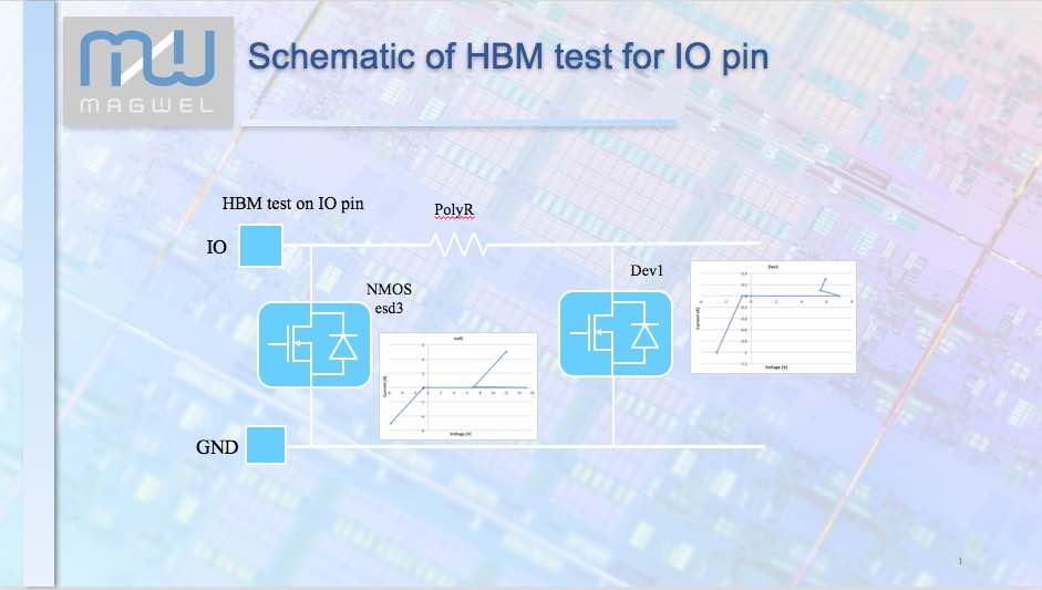
To illustrate the value of having editing capability in the analysis tool we will use a case where there is an HBM simulation error involving a primary and secondary ESD device with a poly resistor to help primary device triggering and limit current flow. After finding the error, the next step is to modify the resistor to alter the resistance, then perform re-simulation to see if the problem is fixed. This is a tricky modification because too high a resistor value can affect input pin behavior. So, the goal is to add just enough resistance to allow the protection to operate properly, but not to overdesign to the point where performance in operational mode is affected.


Figure 1 – Test circuit schematic with TLP models


Figure 2 – Test case in ESDi GUI

In this design, ESD device “Dev1” initially triggers first. However due to the low resistance of resistor “PolyR” of 3.3 Ohms, the primary device “esd3” never triggers. As a result, all of the current for the discharge event travels through Dev1 and the voltage drop across the device reaches 8V, which will lead to device burnout. After the initial simulation, the designer will want to change the area of the resistor to increase the resistance.


Figure 3 – Circuit with ESD violation

Inside of ESDi there is a suite of layout editing commands that allow the designer to modify the layout geometry. Using these commands, it is easy to change the width of the poly resistor and its contacts.


Figure 4 – Editing operation to modify PolyR resistor prior to reanalysis


Figure 5 – After PolyR resistor modification

Once the geometry is changed, the ESD solver can be quickly rerun to perform an HBM simulation on the pad pair in question. With the changes that were made the new simulation results look much better. With the higher R value on PolyR, the primary device triggers, carrying the brunt of the current. Also, the voltage is clamped at a lower value, avoiding device burnout.


Figure 6 – Circuit after fixing violation in ESDi with layout editing commands

After debugging and experimentation, when optimal results have been obtained, the designer can move back to their layout tool and finalize the changes in the original design.

This is why customers say good things about ESDI for saving them considerable time and hassle by enabling them to make changes right in the analysis tool. For ESD integrity it is very important that designers and ESD experts have accurate, effective and easy to use tools. The earlier and more often ESD protection is reviewed, the lower the likelihood that an error or violation will make it through to silicon. Having editing built-in to ESDi makes the process more efficient and provides better results in the form of fewer design iterations and less rework.

More information about Magwel’s ESD solution can be found at their website.


Webinar: Ensuring System-level Security based on a Hardware Root of Trust

Webinar: Ensuring System-level Security based on a Hardware Root of Trust
by Bernard Murphy on 08-23-2018 at 7:00 am

A root of trust, particularly a hardware root of trust, has become a central principle in well-architected design for security. The idea is that higher layers in the stack, from drivers and OS up to applications and the network, must trust lower layers. What does it help it to build great security into a layer if it can be undermined by an exploit in a lower layer? The lowest level foundations of the stack – hardware and bootloader for example – must guarantee trustworthiness in operation; these become the root of trust. The function of this level is to ensure trust in critical functions – trust in downloaded software/firmware, trust in device authentication and trust in the security of privileged operations such as encryption.

REGISTER HERE for this Webinar on September 6th, 2018 at 11:00 AM PT.

Why is this so important? After all, the easiest place to attack is in application software and the beauty of hardware is that it is difficult/impossible to attack, right? Remember there is software, aka firmware, that runs down in the hardware, driving the bootload process for example. Not as easily accessed as application software, particularly if that code is stored in ROM, but not inaccessible either.

One telling example was demonstrated in Nintendo Switch consoles. This depends on a USB recovery-mode offered by the Nvidia Tegra X1 on which the console is based. Maybe you can already guess the problem. This mode can be tricked into bypassing the normal processes to control external data input. This starts by shorting a pin on a controller connector, forcing the USB recovery mode. Then the USB input fakes out the recovery using a variant on the time-honored buffer-overflow exploit; sending a bad length arg can force the system to request up to 64K bytes per request, overflowing the DMA buffer in the boot ROM, from where it can be copied into the protected application stack. From there it can do anything it wants since it’s already privileged. Yikes.

Of course another problem is that ROM coding is pretty final. Great if you know it can never be hacked but see above for how well that worked out for Nintendo (who apparently have already shipped ~15M consoles with this vulnerability). Perhaps a better approach is to accept that we can never guarantee absolute security and instead allow for carefully-secured updates to firmware to address the latest known threats.

The logical way to do this is through over-the-air (OTA) updates. For many reasons, no-one wants to have to plug in a USB-stick (again, see above) or have to visit a dealer/shop for an update. Security updates should be painless; OTA is the only way we know how to do that today. But how many ways could that be compromised? Man-in-the-middle attacks, or faking OEM credentials? These won’t just spoil a game; they may hack your car and since they’re working with a boot image, again they can take over everything. Fortunately, this kind of attack can be largely averted through strong authentication, using encrypted downloads and signing the code in some manner to detect any code-tampering on each boot.

Adding these kinds of root of trust to a system obviously isn’t just a matter of plugging in an extra block of RTL. There are multiple components: CPU, memory, true random number generator, encryption logic and software at minimum. And these have to be configured together with your system needs, providing plenty of opportunities for you to get it wrong in some subtle way.

Meltown, Spectre and more recently Foreshadow may garner the majority of media attention and panic but all devices need a root of trust. Whether you build your own from scratch, from 3[SUP]rd[/SUP] party IP or you use a pre-built ROT solution, you still have to verify correct operation of the ROT. You might want to watch Tortuga’s webinar on this topic. You can REGISTER HERE.


When it Comes to Process Migration, “Standard Cells” are Anything But

When it Comes to Process Migration, “Standard Cells” are Anything But
by admin on 08-22-2018 at 12:00 pm

Standard cell library developers are faced with a daunting task when it is time to create a library for a new process node. Porting an existing library can be a big help, but even then, manual modifications to 800 or more cells is still required. Each of those cells has many geometric elements are that affected by new design rules. All edits and changes have to be adjusted so that the results are DRC clean. In some cases, any advantage coming from reuse might be negated by the amount of effort required for porting.

I recently viewed a webinar by Silvaco on the topic of automating standard cell library porting. Their Cello tool helps with layout migration, layout optimization and standard cell layout creation. Because they use the same tools internally for their standard cell library development and porting services, Cello has evolved based on real world experience. The webinar pretty thoroughly shows how Cello is used to not just to port, but also used to modify cell libraries for specific requirements in areas like Automotive or DFM.

The webinar was hosted by Guilherme Schlinker, Director of Layout Automation at Silvaco. Guilherme made the point early on that in most standard cell libraries there are many cells that might not require special attention, and that there is a smaller set of critical cells that will require hand tuning. Cello frees up skilled library developers to work on the most critical cells while it handles the bulk of the porting effort. Cello has features that include an intuitive GUI cockpit, Tcl scripting, 2D compaction and spacing, built in macros, distributed jobs, and export to GDS, LEF, CDL and LPE. It is integrated with Virtuoso and Custom Complier, or users can use its native layout editor.

The process starts with a proportional scaling of the layout to the new feature size. This is followed by rule specific sizing to ensure that the output is DRC correct. This includes things like enclosure and spacing rules. Additionally, if needed, versions of the cells with increased enclosure can be easily produced for higher reliability applications such as automotive, etc.

Another important element of the porting process is ensuring that there is correct pin accessibility. Silvaco’s Cello takes a unique approach by adding virtual vias and then running DRC checks. In advanced processes via spacing rules can be more restrictive than metal spacing rules. It is painful to learn later that a seemingly DRC correct cell is not usable due to pin accessibility issues. Another interesting application for this technology is in looking at the effect of design rule changes on library performance. It’s relatively straightforward to apply library wide changes and then look at changes in cell or design characteristics.

Also during the webinar Guilherme talked about some of their migration projects. In one instance their Foundation IP Team used Cello to convert ~600 cells from 180nm to 130nm in only 5 days. This included review and fine tuning by a single engineer. He estimated that they benefited from a 10X speed up when compared to manual migration. It’s worth mentioning that Cello works equally well for FinFET processes or planar CMOS.

Fortunately, the webinar is archived on the Silvaco website and available for on-demand viewing. The video goes into much more detail about the user interface, geometry output and the features for controlling the results. I suggest taking a look to get a complete picture of Cello’s capabilities.


The Pain of Test Pattern Bring-up for First Silicon Debug

The Pain of Test Pattern Bring-up for First Silicon Debug
by Daniel Payne on 08-22-2018 at 7:00 am

In the semiconductor world we have divided our engineering talent up into many adjacent disciplines and each comes with their own job titles: Design engineers, Verification engineers, DFT engineers, Test engineers. When first silicon becomes available then everyone on the team, and especially management all have a few big questions on their mind:

  • Is first silicon working?
  • Do we have any functional bugs?
  • Do we have any test program bugs?

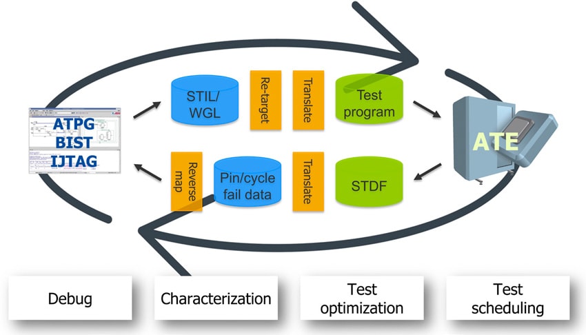
Getting time on an ATE system is a big challenge, because these specialized testers can be pre-booked for other devices and you may just have to wait for your turn to open up in the schedule. Let’s take a look of the silicon bring-up process:

  • DFT engineers create ATPG patterns
  • ATPG patterns converted into tester-specific format
  • Test program runs on the ATE system
  • STDF output file gets translated into failure date
  • Identify failing logic

Here’s a flow-diagram of silicon bring-up and debug:

Another complexity is that your ATPG patterns can be generated at the core level, but then need to be re-targeted to the chip-level. If so, then the failure date needs to be reverse mapped from chip-level to core-level prior to any diagnosis. This flow is complex, takes precious time and can be prone to mistakes.

See how there can be drama between test engineers and DFT engineers, getting time on the tester, or even diagnosing failures between core and chip levels?

There is a natural back and forth between test engineers and DFT engineer during silicon bring-up, so anything to help communicate or cut time in the debug process is certainly welcomed. Mentor did something about improving this situation by creating a new bring-up flow called the Tessent SiliconInsight Desktop flow, and here’s what their setup looks like:

With this approach a DFT engineer can do silicon bring-up using the Tessent Shell environment connected to simple test instruments, USB to digital adaptor and a validation board. Even the test engineers can use this same setup instead of relying upon a complete ATE system. Nobody has to wait for scheduling time on the ATE when using this desktop flow instead. Failure data is readily understandable with the desktop flow using either non-compressed or compressed ATPG patterns, so there’s no long cycles of pattern execution and analysis.

Alternatively you could try a simple JTAG port approach to silicon bring-up, but then you wouldn’t have the flexibility of SiliconInsight Desktop because with it’s non-JTAG test access it can support ATPG patterns with chip compression and more than 25 external scan channels for test and diagnosis. Yes, there is some engineering effort for your team to create the validation board, but it’s a convenient way to allow control of your DUT with simple instruments.

On the software side here’s how you create your tests and diagnose results during bring-up:

Using this flow during silicon bring-up a failure occurs in a test pattern and you want to know which specific scan cells find the failure. If your chip is using on-chip compression and hierarchical DFT then it calls for some sophisticated decoding and dedicated diagnosis patterns. Fortunately for us when using Tessent SiliconInsight all of those details are automated, so we can focus on the analysis part.

Case Study
Cypress Semiconductor shared their actual experience during bring-up of a touchscreen controller chip at the IEEE%20International%20Workshop%20on%20Defects,%20Adaptive%20Test,%20Yield%20and%20Data%20Analysis%20-%20Call%20for%20participation.eml.html”]2016 IEEE Workshop on Defects, Adaptive Test, Yield and Data Analysis. Here’s their setup using Tessent SiliconInsight:

When ATPG patterns were run then a failing cycle was found, and diagnosis pinpointed the suspects as two flops in a scan chain. The engineer was then able to isolate and mask the failing flops, and create a new ATPG pattern set. With the new pattern set the tests passed with no other failures detected. They found the root cause of the silicon failure with this new bring-up flow, all without having to use a costly ATE system and in a much shorter time frame than before.

Conclusion
Silicon bring-up is filled with anguish, pain and pressure, as everyone in the company wants to know how healthy first silicon is looking. Using a new approach called Tessent SiliconInsight Desktop looks to be quite promising because it only requires simple instrumentation, laptop, adapter board and a verification board. Your expensive ATE systems can be used for production requirements, instead of silicon bring-up now. This new flow supports lots of features:

  • Embedded memories
  • Logic
  • IEEE 1687 IJTAG instruments
  • Quick failure mapping
  • Diagnose to failing memory cell, scan cell or net segment

Read the complete six page White Paper online.

Related Blogs


Harnessing Clock and Power

Harnessing Clock and Power
by Alex Tan on 08-21-2018 at 12:00 pm

Switching translates to power. Similar to the recent slow down experienced by Moore’s Law, the constant power density (power demand per unit chip area) prescribed by Dennard scaling was no longer affordable across the technological scaling. While the contribution of leakage power component in advanced process nodes was getting somewhat rectified recently, managing the dynamic power attributed to the increase device density is still a challenge as it is critically demanded by many mobile, IoT and data center applications.

Power, Clock and PowerPro
Dynamic power is defined to be proportional to frequency as given by the equation: ; where k is switching activity, f is design frequency, c is capacitance and Vdd is operating voltage. Aside from memory, the clock network has been the major contributor to the overall power number as it is typically the largest net sprawling across the design and operates at the highest frequency of any signal within the entire synchronous system.

The traditional approach of power saving involves controlling switching of the clock network by inserting clock gating, which can be performed either at the RTL capture stage or during the synthesis stage through logic inferencing. On there other hand, there are many logic implementation styles such as in sharing common enable signals, applying derivative clock trees or free-running clocks, among others, hence, addressing a power optimal clock-tree implementation early is key in order to yield the greatest saving impact and to prevent unnecessary undoing of coded RTL as illustrated in Figure 1.

Since design-for-power methodology demands a rather holistic and converging solution, the availability of a solution that could identify a power optimal RTL code early, accurately assess and propagate the incurred power amount throughout the implementation stage is desirable. Mentor’s PowerPro has an integrated platform addressing such needs.

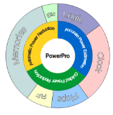
PowerPro has been the solution leader in RTL power optimization domain for the last few years. It provides a complete solution for measuring and optimizing power through an interactive exploration at the microarchitectural level. PowerPro is capable of spotting power leakage and applying opportunistic clock gating insertion during the RTL development cycle, while its physical-aware flow provides the necessary accuracy for estimating design power values. Its guided power reduction includes the recommended RTL codes that would satisfy the power saving and automatically validated by its built-in formal equivalency engine.

Alchip, CTS and Fishbone
Alchip® is a fabless ASIC provider serving various computing market segments and utilizes advanced process nodes to do IC design. In an attempt to further reduce power consumption on high performance designs, they have ventured into applying PowerPro solution on the clock tree implementation.

Clock network implementation can be categorized into two major types. as a tree structure or in gridded/mesh form, with some variations in between. The amount of shared network branches, connecting the a clock driver (root) to the sink points determines if the implementation is closely resembled to the conventional clock-tree network. As part of clock-tree implementation, CTS (Clock Tree Synthesis) is usually presented as an embedded P&R tool function as illustrated in the diagram Figure 2.

A 16nm, 600Mhz core processor design was used as a test vehicle using this flow. Two different clock topologies were applied: a conventional CTS and a fishbone clock tree as shown in Fig. 3. Only the total power numbers of two critical design entities: the flops and design clock network were compared as the power contribution from logic network or memories are effectively unchanged.

Sequential and Memory Clock Gating
Sequential clock gating requires the use of sequential analysis over multiple clock cycles to identify writes that are either unobservable down-stream or the same value is written in consecutive cycles. Deep sequential analysis has enabled PowerPro to take advantage of subtle RTL coding inefficiencies such as unused computations, data dependent function and don’t care cycles. It could disable previous cycle register data generation if data is not used in the current cycle.

Two prominent sequential clock gating techniques adopted by PowerPro: an Observability based Clock Gating in which scenario a change in a signal value does not propagate to a primary output/flop/latch/memory and does not affect the primary outputs (redundant writes that will not be used in subsequent clock cycles).

In the example on Fig.4, the circuit was a three staged pipeline data path containing 5 flip-flops. Under the combinational clock gating condition, only the last flip flop was gated and data flows through two computational stages before being latched into the output register dout. The output of doutis held based on the signal vld_2. Through combinational analysis, the clock gate on doutis added as a simple combinational substitution of the feedback loop. Sequential clock gating on both d_1and d_2requires a sequential analysis to propagate the data hold condition backwards, disabling the unused computations in previous cycles.

As illustrated in Figure 5, the second type is called Stability-based Clock Gating, which is when the same value as in the previous clock cycle is getting latched into a flop/latch such that it will not have any effect on the primary output. Although all of these analyses can be done vector-less, it can take user’s provided activity vectors through various formats (QWAVE, SAIF, FSDB) for further refined results.

Aside from flip-flops, memory components are prone to redundant toggles, as only a few memories are ON at any time. These can be reduced by means of similar coding techniques. The SRAM enable was intentionally left uncontrolled to represent the worst-case scenario for memories. PowerPro showed that it could automatically detect the enable signal and gated the SRAM properly by applying both the Observability-based and Stability-based clock gating –to resolve redundant read and write operation respectively– saving the memory’s dynamic power significantly.

Result Summary
There was an increased of 28% more clock gating covering over 68% of flip-flops compared with only 53% without PowerPro as captured Table 1. The additional clock gating cells did not adversely impact the design, instead it decreased the average toggling percentage on the output of integrated clock gatings (ICG) from 92.7% to 65.1%.

A significant reduction of power was reflected in total power for registers (26% less) and memories (80% less) as shown in the Table 2.

When PowerPro application was combined with the fishbone architecture, the overall impact is more pronounced of 59% total power reduction. Both the pre and post layout power numbers were also shown to correlate well: 31% post-layout vs 26% @ RTL for FF and 86% post-layout vs 80% @ RTL. PowerPro results were produced in the context of the RTL code, schematic display, design hierarchy representation and various sortable reports to enable efficient analysis and easy power tracking throughout the design cycle. It also accommodates the ECO flow by non-disruptive validation of post-ECO generated gate-level netlist to assess power.

Key takeaways from this case study: Mentor’s PowerPro allows power exploration and significant power optimization at micro-architectural level. Its pre-layout/RTL level power estimation shown with Alchip’s testcase to be within 6% compared with post-layout for both memories and sequential cells. The embedded equivalency checking facilitates an optimal RTL code that is correct-by-construction, thus helps ensuring convergence during design implementation. Such process agnostic power optimization should provide good starting point for power sensitive design as we head into 7nm process node and beyond.

For more details on PowerPro check HEREand Alchip case study and others please check HERE.


Computer Vision Design with HLS

Computer Vision Design with HLS
by Bernard Murphy on 08-21-2018 at 7:00 am

I’m on a mini-roll on the subject of high-level design for ML-based systems. No complaints from me, this is one of my favorite domains and is certainly a hot area; it’s great to that EDA vendors are so active in advancing ML-based design. Here I want to talk about the Catapult HLS flow for use in ML design.

Since I’ve covered the ML topic multiple times, I won’t bore you with a lengthy discourse on the basics. ML (at least in this context) is based on convolutional neural nets (CNNs), inspired (somewhat) by the way neurons process information in our brains, starting from a full image and progressing through transformations in layers of operations with coefficients/weights pre-determined by training to ultimately indicate recognition of a trained image.

From a design point of view, this doesn’t look much like regular logic design/architecture, though of course it all winds up in logic functions, primarily multiply-accumulate (MAC) functions, 4-port registers for tightly-coupled memory and SRAM for next-level caching, all most commonly supporting some type of fixed-point representation. But these are leaf-level functions. The layers in a vision CNN may be processing images with 1M+ pixels, each with 24+ bits for color. So the first layer alone has to process a huge number of inputs (down-sampling through later layers will progressively reduce these sizes).

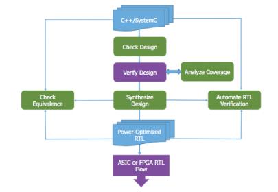
That means you have to use high-level modeling to experiment with architecture choices and to validate your design against real image data. And if you can map your ultimate design to RTL through high-level synthesis (HLS), such as Mentor’s Catapult HLS, so much the better, especially since that tool supports design in straight C++, making it an appealing starting point for people more familiar with algorithms than the intricacies of SystemC (FYI, Catapult HLS also supports SystemC).

Of course if you want to synthesize to a CNN, you’re going to have to accept some limitations on your C++ coding style. For example, you need to use fixed-point data types and you should use fixed-size memory arrays and array indexes, rather than dynamically allocated memory and pointers. Which is not really a problem because you want to do this anyway to reduce power. Mike Fingeroff (HLS Technologist at Mentor) provides guidance (in the white paper link at the end of this blog) on some of the more common areas where you need to adapt.

Taking the HLS path with Catapult HLS offers a number of advantages. The tool can automatically synthesis interface logic (such as AXI4 video stream) based on simple user choices. It will also automatically optimize timing during the synthesis scheduling step, given constraints you set for other factors such as latency and area. In fact in general this is an area where you can experiment with timing versus resource/area tradeoffs based on feedback from the tool. For example you can look at tradeoffs in unrolling loops to drive parallelism. The tool will also help you explore tradeoffs in memory such as word-width and block or interleave choices. And, using PowerPro technology, the tool lets you explore the power implications of all these tradeoffs, so between all these factors you can get to an optimum PPA for your design.

One question occurred to me – how do you bootstrap this process from a trained network with weights? Ellie Burns, Director of Marketing, Calypto Systems Division at Mentor, provided a revealing explanation. It might seem like this is a big deal, but in practice current customers are carrying over the design (and weights) more or less by hand or using their own scripts without difficulty. The much more important need for those teams is the PPA tuning they can get in optimizing microarchitecture choices. Experimenting with options in the synthesis engine and testing/characterizing with real-images/video at the C-level is where they invest the majority of their effort.

Computer vision has become a critical differentiator in many products, but obviously it is not enough that such products support vision. They also need to be fast, very low power and as low cost as possible in many contexts (such as IoT applications). Those are challenging goals; you are adding state-of-the-art functionality but it still needs to fit inside a consumer-acceptable footprint. HLS is an interesting way to get there, by letting you experiment with your algorithm in C++ to optimize and fine-tune the implementation through synthesis. I should add that this flow works both with ASIC-based and FPGA-based designs. You can learn more from this white-paper.


Webinar: NetSpeed is about to change the way SOCs are designed

Webinar: NetSpeed is about to change the way SOCs are designed
by Tom Simon on 08-20-2018 at 12:00 pm

A large part of the effort in designing SOCs has shifted to the integration of their constituent IP blocks. Many IP blocks used in SOCs come as ready to use components and the real work has become making them work together. Network on Chip (NoC) has been a huge help in this task, handling the interconnections between blocks and planning for anticipated traffic. NoCs have evolved quite a bit, becoming more like full blown networks, offering features like QoS, traffic management, cache coherency, high reliability and true layered networking protocols. NetSpeed, a leading provider of NoC technology, is using its foundation technology and a number of innovations to expand their offering to address a much larger part of the job of integrating IP blocks to build an SOC.

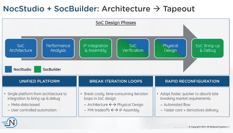
NetSpeed’s NocStudio already helps with making architecture decisions and analyzing performance. It also helps with some aspects of SOC verification and physical design. Their new offering, SocBuilder goes much further by handling IP integration and assembly. Additionally, it compliments NocStudio in the areas of SOC verification and physical design. Even more interestingly it provides support for SOC bring-up and debug. Because SocBuilder and NocStudio share a single platform, they share metadata and can be controlled and automated as a single system.

One of SocBuilder’s key features is the use of reference designs and an extensive IP catalog. Information gleaned from the reference designs and protocol information from the IP catalog are used by machine learning, and advanced data analytics and visualization to assist the design process. Because much of the work during SOC design is related to protocol related issues, this is a ripe area for improved analysis and automation. SocBuilder works with IP descriptions in IPXACT and has extensions for additional metadata for IP. NetSpeed is working with a large number of partners to ensure good coverage of popular IP in their catalog.

With the large array of metadata and IP information available to SocBuilder, it can help with all aspects of physical design, including clock/reset/power, trace/debug/telemetry, MMU/security, and interrupts. These chassis related aspects of the design can be vexing, so having tools to guide the process can be critical to meeting quality goals and deadlines. SocBuilder uses industry standard LEF/DEF during floor planning. SocBuilder assists with connectivity and address map design as well.

After floor planning, system simulations can be run in SocBuilder to ensure performance, power and functional safety goals are met. There is visual feedback for a wide variety of system performance parameters such as power and thermal, etc. The final design is then run through extensive LINT checks that covers protocols, power, connections, performance, etc. System level deadlock checks are also included in SocBuilder.

The outputs are comprehensive. SocBuilder provides SystemC, RTL for the design description. DEF, SDC and scripts are output for the physical design. Test benches are also generated. SocBuilder helps with the essential task of software design too. It produces C models, reference documentation and a programmer’s guide. PPA metrics are also output.

There is an upcoming webinar to acquaint SOC designers with the features and to go into more depth regarding how it works. The Webinar will be on Tuesday August 28[SUP]th[/SUP] at 8AM Pacific Time and registration information is available on the NetSpeed website.I did not dwell much on the machine learning aspect, but this is a reminder that machine learning is in the process of transforming design. Companies that have experience with ML in design and that are expanding its use will certainly be able to make big leaps in enhancing designer productivity.


TSMC GlobalFoundries and Samsung Updates from 55DAC

TSMC GlobalFoundries and Samsung Updates from 55DAC
by Daniel Nenni on 08-20-2018 at 7:00 am

One of my favorite traditions at the Design Automation Conference is the Synopsys foundry events (the videos are now available). I learned a long time ago that the foundries are the foundation of the fabless semiconductor ecosystem and your relationships with the foundries can make or break you, absolutely. I also appreciate the free food, food tastes much better when it’s free.

Synopsys has an advantage being not only the number one EDA company but also the number one IP provider with the largest IP portfolio known to semiconductor man or woman. You can bet Synopsys tools and IP are silicon proven on every edge of the process technology spectrum (leading through trailing) without a doubt. One of the benefits of live events of course is that you get to mingle with the crowd and speakers which includes ecosystem executives from all over the world and don’t be surprised if Aart de Geus or Chi-Foon Chan are breaking bread at your table.

My favorite breakfast of course is the one with my semiconductor bellwether TSMC. Willy Chen, Deputy Director, Design Methodology and Service Marketing, TSMC, is a great speaker and very transparent in what he presented last year versus this year. Willy is a very smart and fashionable guy and very approachable so approach him if the opportunity presents itself. Kelvin Low (Moderator), VP of Marketing, Physical Design Group, Arm is also a great speaker. Kelvin spent the first half of his career with foundries (Chartered, GF, and Samsung) and is now IP. Hopefully next he will go into EDA completing the ecosystem trifecta! Also speaking were Kiran Burli, Director, Solutions Marketing, PDG, Arm and Joe Walston, Principal Engineer, Synopsys.

Designing with Leading-Edge Process Technology, CPU Cores and Tools
Faster, smaller, cooler product requirements continue to challenge designers to achieve their targets. TSMC, Arm and Synopsys kicked off DAC 2018 to share results of their collaboration to address these challenges to enable optimized design and accelerate design closure for Arm®-based designs on the latest TSMC process technology using the Synopsys Design Platform. This event video introduces the new Synopsys QuickStart Implementation Kits (QIKs) for ARM® Cortex®-A76 and Cortex-A55 processors that take advantage of ARM POP™ technology and Synopsys tools, and the collaborative design enablement for TSMC 7-nm process technology.

My beautiful wife joined me for the GlobalFoundries dinner which was focused on FD-SOI. As you know I am a big fan of FD-SOI which we track closely on SemiWiki. In fact, Scotten Jones just did a very nice FDSOI Status and Roadmap last month following SEMICON West. Kripa Venkatachalam, Director of Product Management, GLOBALFOUNDRIES, did a very nice presentation followed by Wayne Dai, President and CEO, VeriSilicon, and Jacob Avidan, SVP of Design Group R&D, Synopsys.

Addressing the Design Challenges of IoT Wearables and Automotive with 22FDX Technology
In this video of the Synopsys and GLOBALFOUNDRIES dinner panel event at DAC 2018, you will hear a discussion of how GLOBALFOUNDRIES’ innovative FDX process coupled with Synopsys’ design tools are providing mobile, IoT and automotive chip designers with the low-power and high-performance technology required for product success. VeriSilicon shared some specific examples of their successes with GLOBALFOUNDRIES’ 22FDX process and Synopsys tools. The event concluded with a panel discussion on various aspects of designing with 22FDX and addressing barriers to adoption of this technology.

Last but not least was the Samsung breakfast featuring Robert J. Stear, Senior Director, Samsung Foundry; JC Lin, Vice President of R&D, Synopsys; and John Koeter, Vice President of Marketing, Synopsys. Samsung has made great ecosystem strides in the past few years and is clearly experiencing the benefits. In fact, Samsung is holding a Tech Day on October 17[SUP]th[/SUP] in San Jose. If you have a golden ticket I hope to see you there. Tom Dillinger and I will be covering it for SemiWiki.

EUV is a very hot topic and Samsung is leading the way with their 7nm EUV process. Scott Jones has also covered Samsung and EUV with Samsung 10nm 8nm and 7nm at VLSIT and SEMICON West – Leading Edge Lithography and EUV
Enabling Optimal Design with Samsung 7nm EUV Process Using the Synopsys Design Platform
As each new process technology brings with it significant advantages as well as design challenges, Samsung Foundry and Synopsys continue to collaborate to enable optimal design. At this event, you’ll learn how our efforts provide a robust foundation for designers to get the most from Samsung advanced process technologies using Synopsys’ Design Platform with Fusion Technology and state of the art IP.

Take a look at the videos and let’s talk foundries in the comment section…