webinar banner AI 2026 v2

AMAT down 10% as expected Foundry spending slow down unexpected

AMAT down 10% as expected Foundry spending slow down unexpected
by Robert Maire on 08-19-2018 at 12:00 pm

Applied reported a more or less in line quarter, slightly beating weaker expectations. As we had projected, the October quarter is expected to have revenues down 10% which is at the low end of our expected 10-15% drop in business. Applied services helped partially make up for some of the equipment sales weakness. Revenue came in at $4.47B versus street of $4.43B and EPS was $1.20 versus street $1.17. The October quarter is guided to $4B and EPS of $0.96 versus $4.46B and $1.17. Its clear that most analysts neglected to cut their numbers despite the widespread news.

Similar to what we heard from both Lam and KLA, management suggested Sept/Oct quarter would be a trough. However we were slightly surprised that management refrained from describing what the recovery might look like, and how long we would be in the trough. This is a sharp variation from KLAC which called for a “sharp snapback” and even weaker than Lam’s vague and softer, “positive trajectory” comments.

Perhaps one of the reasons for the weaker and less committed outlook is that Applied revealed on the call that the weakness in spending which had been limited to Samsungs memory side has now spread to foundry customers. Thats customers with an “S” as in more than one foundry is slowing down their spending.

We can only assume that both TSMC and Samsung are slowing their foundry spend as they are the biggest foundries and GloFo isn’t spending that much to start with. This seems to be somewhat confirmed as the mix of foundry business has been shifting from leading edge to trailing edge spend. The company still feels very bullish about 2019 being up in spend but we think its going to be very hard to get there from here if both memory at Samsung and at least two foundry customers are slowing their spend.

Its also clear that there is not an expectation of a rescue coming in from the display side of the business. The part of the business that’s doing a great job continues to be Applied’s services business which is helping to offset weakness in new tool sales. It’s clear to us that the reduced cyclicality is as much a reflection of a higher services business as it is a reflection of more rational spending

Potential share loss???
In doing the math of AMATs tool business against global WFE spend is seems as if AMAT is losing share as its revenue, as quoted on the call, is not growing as fast as the industry top line. Management danced around without directly answering a question on the call on the share loss math. This could be due to the predominance of memory spending we have seen where AMAT has a lower share.

2019 Outlook

Management doubled down on their outlook for 2019 by saying that 2018 and 2019 will now exceed $100B where they had previously just said $100B. If the October and January quarters are weak in 2018 we can see how 2019 could be better but we are more dubious of what will now have to be higher growth in 2019 to make the numbers work, especially in light of BOTH memory and foundry being weaker.

Handset Weakness?
We had previously mentioned our concern about Samsung’s potential plan to shutter a China handset factory. We think this could be evidence of further slowing which manifested itself as a slow down in foundry spend at both TSMC and Samsung that would obviously have been making chips for the factory that is to be shut.

The Stock
Investors obviously did not like the lower outlook and the spread of weakness to now include foundrieS, as the stock was off over 4% in the after market. We would imagine that this new, added concern about foundry spending will likely weigh on the group as a whole tomorrow. We had also been hoping for a stronger rebound statement that would show some hard evidence or confidence in the speed of some sort of recovery but that was also missing on the call. Applied results coupled with less than stellar news out of Nvidia could spread to other semi names and we could see the overall group weaker as well.

Also Read: Chip Stocks have been Choppy but China may return


Chip Stocks have been Choppy but China may return
Chip Stocks have been Choppy but China may return

by Robert Maire on 08-19-2018 at 7:00 am

Applied Materials (AMAT) is batting clean up in a quarter that has not been pretty. Lately semi stocks seem to have been hit by not only stock specific issues but continued and increasing memory concerns coupled with more macro issues. On top of all this, China trade issues which have in the meantime taken a back burner to other issues threaten to boil over yet again.
Continue reading “Chip Stocks have been Choppy but China may return”


Measuring Up 7nm IP

Measuring Up 7nm IP
by Daniel Nenni on 08-17-2018 at 12:00 pm

The Linley Group is an industry-leading source for independent technology analysis of semiconductors for networking, communications, mobile, and data-center applications. Their Microprocessor Report is widely read as a source of un-biased, no-nonsense analysis of technologies and trends. So, when they dig into something it’s worth reading.

Mike Demler recently did a piece on eSilicon entitled “eSilicon 7nm SerDes Hits 56GBPS – NeuASIC Platform Includes AI Accelerators for 2.5D/3D ICs”. I know Mike, and he’s one of those “just the facts” kind of guys that speaks from experience, absolutely. I have a copy and here is a quick summary with a link to the report:

The report spends some time reviewing eSilicon’s 7nm SerDes IP. This one IP block has become Star IP for many customers. It implements high-speed serial communication between chips and it’s performance is critical to achieving the overall throughput needed for advanced ASICs. The report goes into some detail about eSilicon’s 56G SerDes – its programmability to allow designers to tune power and performance for long or short reach channels for example. Several other performance statistics about eSilicon’s SerDes are also disclosed in the report.

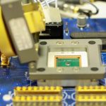
eSilicon’s 56G SerDes test chip on the bench

eSilicon’s HBM2 PHY is also discussed. This IP implements the physical channel between an ASIC and HBM2 memory stacks. It’s available for a variety of technologies and foundries. The use of this IP to implement 2.5D designs with integrated HBM2 memory stacks on a silicon interposer is also discussed. eSilicon’s line of content-addressable memories are also reviewed in some detail, including application scenarios and performance comparisons with other vendors. The report also delves into eSilicon’s platform focus for its IP offerings, with specific packages for AI and high-performance networking. The details of what goes into a high-performance networking chip are discussed. The methodology eSilicon uses to create platform-based AI chips is also reviewed in some detail.

The report concludes with a frank assessment of market dynamics for the highly competitive networking and AI markets – where eSilicon fits well, and what challenges they will likely face. I believe companies like eSilicon that both develop IP and use the same IP for their ASIC business have a built-in advantage in terms of proven IP quality. As part of my research, I hear all of the bad IP stories from the top semiconductor companies and the foundries. IP really is critical and silicon-proven IP is quite valuable. This Linley report is definitely worth reading. You can download a free copy from the eSilicon website.

Also read: eSilicon and SiFive partner for Next-Generation SerDes IP

About eSilicon
eSilicon is an independent provider of complex FinFET-class ASICs, market-specific IP platforms and advanced 2.5D packaging solutions. Our ASIC+IP synergies include complete 2.5D/HBM2 and TCAM platforms for FinFET technology at 16/14/7nm as well as SerDes, specialized memory compilers and I/O libraries. Supported by patented knowledge base and optimization technology, eSilicon delivers a transparent, collaborative, flexible customer experience to serve the high-bandwidth networking, high-performance computing, artificial intelligence (AI) and 5G infrastructure markets. www.esilicon.com

About The Linley Group
The Linley Group is the industry’s leading source for independent technology analysis of semiconductors for networking, communications, mobile, and data-center applications. The company provides strategic consulting services, in-depth analytical reports, and conferences focused on advanced technologies for chip and system design. The Linley Group also publishes the weekly Microprocessor Report. For insights on recent industry news, subscribe to the company’s free email: Linley Newsletter. www.linleygroup.com


Why Do Brilliant People Like to Work Together?

Why Do Brilliant People Like to Work Together?
by Daniel Nenni on 08-17-2018 at 7:00 am

This is the eleventh in the series of “20 Questions with Wally Rhines”

In high technology, there are numerous instances of highly productive groups coming together and generating game-changing ideas and products. This happened at Shockley Semiconductor in the 1960s when Gordon Moore, Bob Noyce, Jean Hoerni and more found each other and took advantage of Sherman Fairchild’s offer to start a semiconductor company. It also happened to me in Houston, Texas in 1978 (a much less likely place than Palo Alto, California).

As related in previous blogs, TI had a late start in the microprocessor contest, focused its attention on calculator chips, and was left behind by Intel and Motorola in the general purpose host microprocessor business. But failure has a way of stimulating the desperation needed for success and the group in Houston went on to develop the TMS 320, the first really successful single-chip DSP, and a host of other important technologies.

Although TI arguably has the original microprocessor patent (awarded to Mike Cochran and Gary Boone), the MOS Division was struggling just to produce MOS Memory and the Microprocessor group was focused on a strategy that would catch up with Intel by second-sourcing the 8080A, develop TI’s own set of 8-bit microprocessors and peripherals (the 5500 series) and then leapfrog with the TMS 9900 16-bit chip that would also be used by the computer and defense businesses of TI
( https://spectrum.ieee.org/tech-history/heroic-failures/the-inside-story-of-texas-instruments-biggest-blunder-the-tms9900-microprocessor ).

Brilliant junior designers like Kevin McDonough and Karl Guttag were involved in the process when I arrived in October 1978. The group was in melt-down mode because the 16-bit microcontroller, called the TMS 9940, was in its sixth or seventh re-spin and looked like it would never work. Although good engineers were resigning at a rapid rate, we had a group in Bedford, England that had just been started. This was the first case I know of where design teams were organized around the world to do 24 hour per day design, with groups of engineers assigned to a particular product in Japan, England and the U.S. could, if needed, pick up the work of each other as the sun moved around the globe and the databases remained in our IBM 4341 or IBM 7090-600 computers.

The Bedford, England design group, was assigned the task of developing peripheral chips for the TMS 9900 16-bit microprocessor. The most notable was the TMS 9914 which implemented the HP GPIB standard. The chip became a long term success despite the lack of success for the TMS 9900. The team even anticipated the risk that others would copy their chip so they went to great lengths to disguise the transistors, making enhancement mode devices look like depletion mode, just to confuse anyone who tried to copy.

A small group was assigned responsibility to develop a graphics chip for the TI Home Computer (https://spectrum.ieee.org/tech-history/heroic-failures/the-texas-instruments-994-worlds-first-16bit-computer ). While the TI 99 Home Computer was a disaster, the chip was not. It led to development of new concepts in graphics and became part of a standard known as MSX that was promoted by K. Nishi, CEO of ASCII Microsoft and was used by more than twenty different computer and video game manufacturers. Many people in graphics development are still familiar with the term “sprites”, a graphical representation that was developed by the TMS 9918 team. This same group went on to develop the TMS 340 graphics processor that was adopted by IBM for the 8514A standard that, unfortunately, experienced a short life before being replaced by VGA in the IBM PC.

About a year after I arrived in Houston (from my previous job as Engineering Manager of Consumer Products in Lubbock), we combined all the logic design resources in Houston under one manager, Jerry Rogers. Jerry had been a career enlisted man in the Navy and joined TI after retirement as a technician while he worked on his engineering degree at the University of Houston. He was an effective manager but very tough, with no sympathy for any performance less than the best. He had a thick skin and was willing to push back on management, a trait that helped with many successes. Later Jerry founded Cyrix, a very successful floating point processor and X86-compatible microprocessor company, and eventually married Jodi Shelton, Founder and CEO of GSA.

During this period in Houston, we hired an amazing array of innovative engineers. TI started a program to train new sales application engineers by assigning them to short stints in the product divisions. Rich Templeton was one of those early assignees. We liked him so well that we convinced him to join our group and give up the rotational training program and he did. Later he became Chairman & CEO of TI. K. Bala was his supervisor. One day in about 1991, Bala mentioned in a conversation with me that he thought one of his employees might be his future supervisor. “Who is that?”, I asked. “Rich Templeton, and I think he might be your boss as well”, said Bala.

Over the years, people who started their careers in that group in Houston eventually managed much of the company. We needed a marketing manager for DSPs when David French (later CEO of Cirrus Logic) was running the business so we brought in Mike Hames who was in the Bipolar PROM group and knew nothing about DSP. When Dave French left to join Don Brooks at Fairchild, we brought in John Scarisbrick to manage the DSP business and he later took it to new heights.

One of the most impressive capabilities came when we needed improved manufacturing. Yukio Sakamoto, the most capable operations manager I’ve ever known, joined us to run all the manufacturing operations. He was dissatisfied with our status and so he promoted Kevin Ritchie multiple levels to the job of DMOS 4 Wafer Fab Manager. People tell me that Kevin became one of the most effective manufacturing managers in the semiconductor industry and recently retired after a distinguished TI career as Senior VP of Technology and Manufacturing. Sakamoto became CEO of Elpida Memory, the company that combined NEC’s and Hitachi’s DRAM businesses.

The 20 Questions with Wally Rhines Series


Networking trends for Automotive ADAS Systems

Networking trends for Automotive ADAS Systems
by Daniel Payne on 08-16-2018 at 12:00 pm

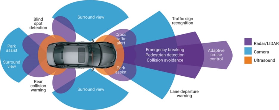
From my restaurant seat today in Lake Oswego, Oregon I watched as an SUV driver backed out and nearly collided with a parked car, so I wanted to wave my arms or start shouting to the driver to warn them about the collision. Cases like this are a daily occurrence to those of us who drive or watch other drivers on the road, so the promises of using Advanced Driver Assistance Systems (ADAS) is especially relevant in keeping us alive and injury free. I did some online research to better understand what’s happening with the networks used in automotive applications.

Automotive networks are tasked with moving massive amounts of data to process and help make decisions, just think about the data that these safety features and systems require:

  • Emergency braking
  • Collision avoidance with other vehicles
  • Pedestrian and cyclist avoidance
  • Lane departure warning
  • HD cameras
  • Radars
  • LIDARs
  • Fully autonomous driving

Our electronics industry is often driven by standards committees, and for networking in ADAS applications we thankfully have the Time Sensitive Networking (TSN) IEEE working group that has thought through all of this and come up with standards and specifications. So let’s take a closer look at how the Ethernet TSN standards can be used in automotive scenarios, then ultimately why you would use automotive-certified Ethernet IP in your SoC design.

Going back to 2005, there was an Ethernet standard for Audio Video Bridging (AVB) used for things like automotive infotainment and in-vehicle networking. These applications aren’t really all that time critical and the data volume was low in comparison to higher-demand tasks like braking control, so in 2012 the IEEE revamped things a bit by transforming this AVB working group into TSN. So with TSN we now have a handful of very specific standards to deal with ADAS requirements:

[table] style=”width: 500px”
|-
| TSN Standard
| Specification Description
|-
| IEEE 802.1Qbv-2015
| Time-aware shaper
|-
| IEEE 802.1Qbu-2016
IEEE 802.3br-2016
| Preemption
|-
| IEEE 802.1Qch-2017
| Cyclic queuing and forwarding
|-
| IEEE 801.1Qci-2017
| Per stream filtering and policing
|-
| IEEE 802.1CB-2017
| Frame replication and elimination
|-
| IEEE 802.1AS-REV
| Enhanced generic precise timing protocol
|-

Time-Aware Shaper
An engineered network will provide a predicted, guaranteed latency. They do this with a time-aware shaper that allows scheduling so that critical traffic gets a higher priority. As an example consider four queues of data, so the IEEE 802.1 Qbv scheduler controls which queue goes first (shown in orange) and so on.

Preemption
In the next example, Queue 2 in orange starts transmitting its frame first, but then a higher priority happens and Queue 3 in green preempts, so in the lower timing diagram we see how the green frame travels ahead of the orange frame. The green frame which is time-critical has preempted the orange frame, providing a predictable latency.

Cyclic Queuing and Forwarding
To make network latencies across bridges more consistent regardless of the network topology there’s a technique called Cycling Queuing and Forwarding. The complete specification is on the IEEE 802 site. Shown below in dark blue is a stream with the shortest cycle packet, while in light blue is a stream in the presence of multiple packets.

Frame Replication and Elimination
How do you find and fix from: cyclical redundancy check (CRC) errors, opens in wires, and flakey connections? With frame replication and elimination. In the following example there’s a time-critical data frame sent along two separate paths, orange and green, then where they join up, any duplicate frames are removed from the streams, so applications can receive frames out of order.

In the IEEE specification there are three ways to implement frame replication and elimination:

  • Talker replicates, listener removes duplicates
  • Bridge replicates, listener removes duplicates
  • Bridge replicates, bridge removes duplicates

Enhanced Generic Precise Timing Protocol
Knowing what time it really is across a network is fundamental, so synchronizing clocks comes up and this protocol lets you use either a single grand master or multiple grand masters, as shown in the next two figures:


Single grand master, sending two copies


Two grand masters, each sending two copies

Each of these TSN specifications have grown over time in order to meet the rigors in automotive design to support real-time networking of ADAS features.

Summary
Ethernet in automobiles has come a long way over the past decade, and now we have TSN to enable the ADAS features of modern SoCs, inching towards autonomous vehicles. With Ethernet in the car we get:

  • Wide range of data rates
  • Reliable operation
  • Interoperability between vendors
  • TSN to standardize on how data travels with predictable latency

SoCs for automotive also need to meet the functional safety standard ISO 26262 and AEC-Q100 for reliability. In the make versus buy decision process for networking chips you can consider IP from Synopsys, like their DesignWare Ethernet Quality-of-Service (QoS) IP because it is ASIL B Ready ISO 26262 certified.

John Swanson from Synopsys has written a detailed Technical Bulletin on this topic.


Chip, Package, System Analysis – A User View

Chip, Package, System Analysis – A User View
by Bernard Murphy on 08-16-2018 at 7:00 am

While I missed ANSYS (and indeed everyone else) at DAC this year, I was able to attend the ANSYS Innovation Conference last week at the Santa Clara Convention Center. My primary purpose for being there was to listen to a talk by eSilicon which I’ll get to shortly, but before that I sat through a very interesting presentation on the growing importance of simulation in validating medical devices. This isn’t the kind of simulation we usually discuss; these are computational fluid dynamics (CFD) sims for blood flow through stents, insulin flow from insulin pumps and other such worthy objectives. ANSYS has a representative on an FDA advisory committee exploring increased use of simulations in regulation for medical devices. Important and fascinating stuff and a reminder of how broadly ANSYS impacts technology in many areas beyond electronic design.


Back to the main topic, eSilicon gave a presentation at the conference on their work with ANSYS to validate signal and power integrity in designs for eSilicon customers. You should understand first that eSilicon works with customers on the leading-edge of custom ASIC design, from HPC to networking, AI and 5G infrastructure. I wrote recently about their platform-specific offerings for AI and networking at 7nm in advanced 2.5D packaging options with high-bandwidth memory stacks. Point being that this is bleeding-edge design for system customers demanding total system performance, not just “the chip works to spec”. So, these designs are a good test for the ANSYS “chip-package-system” (CPS) mantra.

eSilicon doesn’t build the boards. Their customers do that, so they work collaboratively to extract, analyze and optimize the board design together with the ASIC package, interposer and components on the interposer. The speaker, Teddy Lee from eSilicon, detailed flows they used for signal integrity (SI), DC power integrity (PI) and AC power integrity. For signal integrity they extract 3D models from the MCM database into the ANSYS HFSS tool and from this build S-parameter models for insertion loss, return loss and crosstalk, then optimize traces, materials, spacing, etc. and iterate. They do this for the substrate layout and the interposer design, then connect the 2 models and send to the customer for use in their IBIS-AMI channel analysis.


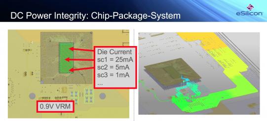
In DC power integrity, customers want to model DC voltage drop from the voltage regulator module (VRM) on the board, through trace and then through the package. Here a customer will again use SIwave to build a model, with IR drop and current densities, which eSilicon combines with a similar model extracted from the package substrate and the silicon interposer and then runs a DC simulation with SIwave. You can see simulated voltage gradients from the VRM to the package in the first figure and from the substrate up through the interposer in the picture above. This clearly provides very fine-grained analysis of power distribution all the way from the voltage regulator on the board up to the die ports.

In Teddy’s view, this system to die view, with accurate extraction at all levels, is essential to getting reliable PI analysis down to the die. He noted that you can’t just assume an idealized VRM somewhere on the PCB. You have to define where it’s going to sit and extract the real traces though which it will ultimately drive the package – the PI analysis you get from the idealized model may be quite different from the real model.

Teddy wrapped up with an explanation of their approach to AC power integrity where they want to look at the impact of noise generated by the die or on the board (everything looks good at DC, but what happens when a power domain turns on or another device on the board suddenly becomes active?). Here they use RedHawk to build a chip power model for the die and interposer, then combine that with an SIwave model for the package substrate and board. Based on this they do a system-level simulation (PCB down to the die) and perform a frequency domain simulation to see where they should add package-level decaps to reduce system-level resonances at the package. This is followed by a time-domain analysis looking at noise on the die. Depending on how this turns out, they may feed that back to the frequency domain analysis where they can change some of those decaps or perhaps change some trace geometries. And again iterate.

So, it looks like eSilicon sees value in CPS-style iterative analysis for SI and PI, given the demanding expectations of their customers. Chalk up another proof-point for CPS. You can learn more about CPS analysis HERE.


Enabling Complex System Design Environment

Enabling Complex System Design Environment
by Alex Tan on 08-15-2018 at 12:00 pm

Deterministic, yet versatile. Robust and integrated, yet user-friendly and easily customizable. Those are some desirable characteristics of an EDA solution as the boundaries of our design optimization, verification and analysis keep shifting. A left shift driven by a time-to-market schedule compression, while the process and application complexities keep pushing it in the opposite direction.

From the many DAC held technical sessions, early verification has made progress in doing shift-left to keep pace with the implementation process by means of integrating the application or end-product software within the virtual prototyping to do an early system design exploration. Virtual prototyping allows designers to not only explore corner scenarios but also to reproduce the experiments with various permutations of constraints or variants. The more heterogeneous SoCs for the emerging applications demand virtual prototyping that supports not only software and hardware but also the incorporation of digital, analog and interconnect IPs.

Magillem provides robust front-end design XML based solutions that enable and streamline design activities around its integrated environment. It has deployed its products across several industry boundaries –from SoC design houses, semiconductor manufacturers to legal and technical documentation publishers.

Since rolling out its Magillem Architectural Intent (MAI) for architectural intent capture as covered in my prior blog, the company has announced a joint effort with Imperas for an integrated virtual prototyping platform and also introduced Magillem Flow Architect (MFA), a turnkey solution that help customers define their best recommended flow.

At DAC 2018, I had the opportunity to interview Magillem CEO, Isabel Geday, and Magillem VP of Strategic Account Manager, Paschal Chauvet. The discussion was centered around Magillem continued efforts to accommodate IC design needs and how it adapts with the current trends in the EDA ecosystem.

Some EDA players have announced their product collaborations. Does Magillem have similar efforts?
“I call it a partnership, by not creating duplicated solutions,” said Isabel diplomatically. She gave example of Magillem’s earlier partnership with Imperas using its Verification IP models and debugging software. At DAC, Magillem announced another partnership with Arteris IP, an indisputable leader in NOC-IP that provides SoC cache interconnect solution.

The integration with Arteris IP was demonstrated by a full-compliance validation of the company’s interconnects with the Magillem environment. Using a single design environment, customers can now easily build a SoC using Arteris’ IP instances (FlexNoC and NCore) and the Magillem front-end design environment (MAI, MPAand MRV). “It is very good for customers to have one design environment. To be able to work with and plug all the IPs,” she added.


Since Magillem is based on the industry standard IP-XACT, it enables a possible integration of other tools into its environment. “While the other big players have closed environments, for Magillem it is the DNA of our product to allow integration,” she pointed out. Furthermore, The unified environment also provides more efficient and automated sharing of information across the supply chain during the product development.

There are increasing AI and ML related efforts. How do these impact your products?
“This is very interesting question as we work with methodology and flow aspects,” Isabel said. She gave two examples. The first is from a product application stand point. A large customer has used Magillem solution on some kind of expert system, which interacts with engineers through questionnaires and depending on the given answers make decisions one way or another.

The second example is related to Magillem prior internal effort. “We had activities on the side, done several years ago to demonstrate how versatile is our platform, by building something using the assembly of metadata of descriptions.” She elaborated that the team applied some AI aspects to analyze the interpreted legal texts and the impact of changes made on the existing document corpus. It measured the impacts of the new text fragments on the existing ones and suggested changes when it’s necessary on the existing document corpus. In addition, it was capable of learning a new syntax, when it did not recognize a new pattern. To sum up, she believes that AI is more a replay of previously exercised concept, but with more memories, compute power and algorithms involved.

Aside from these examples, the recently announced Arteris IP-and-Magillem integrated solution has been targeted to simplify the increasingly complex SoCs designs for AI and autonomous driving applications, which are now bounded by the latency of on-chip interconnects rather than the performance of on-chip processors and hardware accelerators.

Here at DAC, more EDA vendors showcasing their products to be accessible on the cloud. What is your take on cloud deployment?
“Our customer are Tier-1 companies and they have entrusted us with their most complex, expensive, demanding SoC platform and designs,” said Isabel. She added that the customers policy is to keep confidentiality as a top-priority. She acknowledged that although some design data intelligence may benefit from cloud based scenario, cloud is not an option yet. “People gain ownership on this internal solution. It is less interesting idea to us than in providing a cognitive assistance to the experts. The customers are very good on what they do. They have to be the decision maker…to make fast decision and be more productive as they deal with huge legacy and data.”

What is your data model? Do you allow customer flow customization?
“Our solution was directly derived from IP-XACT, which is universal inside our tool, allowing our customers to use one data model for the entire design flow,” said Paschal. Embedding external tools can be achieved through the Eclipse plug-in and TGI (Tight Generator Interface), the standard API to manipulate any IP-XACT database. According to Paschal, such flexibility is crucial for smaller companies as they tend to highly customize their environment. The scalability of the compact data model is not an issue as Magillem have worked with SoC having millions of gates.

Traceability is about the ability to track the safety requirements from the initial design inception through its implementation and operation phase. It is a key ingredient for the functional safety standards compliance as defined in IEC 61508 and ISO 26262. With the parsable IP-XACT based data, automated traceability throughout the development flow can be achieved.

Commenting on future works, Isabel stated that the current Magillem platform offering is unique. “Our earlier vision is now very appealing to new customers and new markets,” she added. Ongoing works includes the infrastructure to build the hub of link that will guarantee traceability in a very elegant way. She added that instead of building a hub of data, one then could add different standards and other sort of data while preserving all the essential elements.

By providing a versatile framework that could be retargeted for complex system designs, Magillem solution enables design teams to adapt with changing requirements from both design specifications and implementation methodologies.

For further info on Magillem products, please check HERE.


What Silicon Valley still gets wrong about innovation

What Silicon Valley still gets wrong about innovation
by Vivek Wadhwa on 08-15-2018 at 7:00 am

Silicon Valley well exemplifies the saying “The more things change, the more they stay the same”. Very little has changed over the past decade, with the Valley still mired in myth and stale stereotype. Ask any older entrepreneurs or women who have tried to get financing; they will tell you of the walls they keep hitting. Speak to VCs, and you will realize that they still consider themselves kings and kingmakers.

With China’s innovation centers nipping at the Valley’s heels, and with the innovation centers that Steve Case calls “the rest” on the rise, it is time to dispel some of the myths by which it operates.

Myth #1. Only the young can innovate

The words of one Silicon Valley VC will stay with me always. He said: “People under 35 are the people who make change happen, and those over 45 basically die in terms of new ideas”. VCs are still looking for the next Mark Zuckerberg.

The bias persists despite clear evidence that the stereotype is wrong. My research in 2008 had documented that the average and median age of successful technology company founders in the U.S. is 40. And several subsequent studies made the same findings. Twice as many of these founders are older than fifty as are younger than 25; twice as many, over sixty as are under twenty. The older, experienced, entrepreneurs have the greatest chances of success.

Don’t forget that Marc Benioff was 35 when he founded Salesforce.com; Reid Hoffman, 36 when he founded LinkedIn. Steve Jobs’s most significant innovations at Apple — the iMac, iTunes, iPod, iPhone, and iPad — came after he was 45. Qualcomm was founded by Irwin Jacobs, when he was 52, and by Andrew Viterbi, when he was 50. The greatest entrepreneur today, transforming industries including transportation, energy, and space, is Elon Musk; he is 47.

Myth #2. Entrepreneurs are born, not made

There is a perennial debate about who can be an entrepreneur. Jason Calacanis proudly proclaimed that successful entrepreneurs come from entrepreneurial families and start off running lemonade stands as kids. Fred Wilson blogged about being shockedwhen a professor told him that you could teach people to be entrepreneurs. “I’ve been working with entrepreneurs for almost 25 years now,” he wrote, “and it is ingrained in my mind that someone is either born an entrepreneur or is not.”

Yet my teams at Duke and Harvard had documented that the majority, 52 percent, of Silicon Valley entrepreneurs were the first in their immediate families to start a business. About 39 percent had an entrepreneurial father, and 7 percent had an entrepreneurial mother. (Some had both.) Only a quarter of the sample we surveyed had caught the entrepreneurial bug when in college. Half hadn’t even thought about entrepreneurship even then, and they had had little interest in it when in school.

Useful specific instances are the backgrounds of Mark Zuckerberg, Steve Jobs, Bill Gates, Jeff Bezos, Larry Page, Sergey Brin, and Jan Koum. They didn’t come from entrepreneurial families. Their parents were dentists, academics, lawyers, factory workers, or priests.

Anyone can be an entrepreneur, especially in this era of exponentially advancingtechnologies — in which a knowledge of diverse technologies is the greatest asset.

Myth #3. Higher education provides no advantage

Peter Thiel made headlines in 2011 with his announcement that he would pay teenagers $100,000 to drop out of college. He made big claims about how these dropouts would solve the problems of the world. Yet his foundation failed in that mission and quietly refocused its efforts and objectives to provide education and networking. As Wired reported, “Most (Thiel Fellows) are now older than 20 and some have even graduated college. Instead of supplying bright young minds with the space and tools to think for themselves, as Thiel had originally envisioned, the fellowship ended up providing something potentially more valuable. It has given its recipients the one thing they most lacked at their tender ages: a network”.

This came as no surprise. Education and connections are essential to success. As our research at Duke and Harvard had shown, companies founded by college graduates havetwice the sales and twice the employment of companies founded by others. What matters is that the entrepreneur complete a baseline of education; the field of education and ranking of the college don’t play a significant role in entrepreneurial success. Founder education reduces business-failure rates and increases profits, sales, and employment.

Myth #4. Women can’t succeed in tech

Women-founded firms receive hardly any venture-capital investments, and women still face blatant discrimination in the technology field. Despite the promises of tech companies to narrow the gap, there has been insignificant progress.

This is despite the fact that according to 2017 Census Bureau Data, women earn more than two-thirds of all master’s degrees, three-quarters of professional degrees, and 80 percent of doctoral degrees. Not only do girls surpass boys on reading and writing in almost every U.S. school district, they often outdo boys in math—particularly in racially diverse districts.

Earlier research by my team revealed that there are also no real differences in success factors between men and women company founders: both sexes have exactly the same motivations, are of the same age when founding their startups, have similar levels of experience, and equally enjoy the startup culture.

Other research has shown that women actually have the advantage: that women-led companies are more capital-efficient, and venture-backed companies run by a woman have 12 percent higher revenues, than others. First Round Capital found that companies in its portfolio with a woman founder performed 63 percent better than did companies with entirely male founding teams.

Myth #5. Venture Capital is a prerequisite for innovation

Many would-be entrepreneurs believe that they can’t start a company without VC funding. That reflected reality a few years ago, when capital costs for technology were in the millions of dollars. But it is no longer the case.

A $500 laptop has more computing power today than a Cray 2 supercomputer, costing $17.5 million, did in 1985. For storage, back then, you needed server farms and racks of hard disks, which cost hundreds of thousands of dollars and required air-conditioned data centers. Today, one can use cloud computing and cloud storage, costing practically nothing.

With the advances in robotics, artificial intelligence, and 3D printing, the technologies are becoming cheaper, no longer requiring major capital outlays for their development. And if entrepreneurs develop new technologies that customers need or love, money will come to them, because venture capital always followsinnovation.

Venture Capital has become less relevant than ever to startup founders.

For more, follow me on Twitter: @wadhwa and visit my website: www.wadhwa.com


Meeting Analog Reliability Challenges Across the Product Life Cycle

Meeting Analog Reliability Challenges Across the Product Life Cycle
by Daniel Payne on 08-14-2018 at 12:00 pm

Create a panel discussion about analog IC design and reliability and my curiosity is instantly piqued, so I attended a luncheon discussion at #55DAC moderated by Steven Lewis of Cadence. The panelists were quite deep in their specialized fields: Continue reading “Meeting Analog Reliability Challenges Across the Product Life Cycle”


Architecting an ML Design

Architecting an ML Design
by Bernard Murphy on 08-14-2018 at 7:00 am

Discussion on machine learning (ML) and hardware design has been picking up significantly in two fascinating areas: how ML can advance hardware design methods and how hardware design methods can advance building ML systems. Here I’ll talk about the latter, particularly about architecting ML-enabled SoCs. This approach is getting major traction for inferencing applications particularly when driven by power considerations (eg in the IoT and increasingly in automotive apps), also in training when driven by demand for highest performance per Watt (eg Google TPU).

Architecture has to be the center of design in such a system, optimizing the algorithm and architecture for your CNN. For the core algorithm, this has to be in choice of number, types (convolution, pooling, …) and characteristics (stride, …) of layers in the network. In the implementation, memory support is one critical consideration. Neurons like tightly-coupled memories for weights, activation functions and retrieving and storing neuron inputs and outputs, but everything can’t be tightly-coupled so you also need high-bandwidth access to larger memories – like caching but implementation can be quite different in CNNs. And you want to optimize PPA, aggressively if the design is targeted to a battery-operated application.

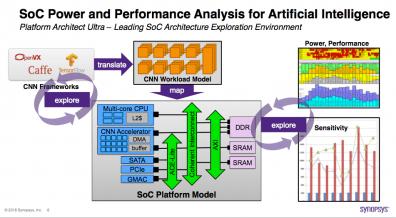
There are challenges in finding an optimal architecture for these systems. RTL isn’t an option – you need to test out different options with 100’s of MB of data (images as an obvious example) so this has to run at a higher level of abstraction. And it’s not obvious (to me at least) how you would experiment with CNN architectures in a JIT-type virtual-prototype running on a general-purpose processor (or even a cluster). This class of architecture design seems a much better fit with TLM approaches, for example Platform Architect Ultra.

You’ll likely start in one of the standard CNN frameworks (Caffe, TensorFlow, etc) where most experts in the field are familiar with building CNN graphs. You can translate this into a workload model in Platform Architect (Synopsys calls this a task graph). This can then be mapped into an IP in your larger SoC model: CPUs, memory interfaces and on-chip bus. Naturally the platform supports a rich library of IPs and VIPs for this task:

  • Processors – Arm, Synopsys ARC, Tensilica and CEVA DSP, traffic generators and more
  • Memory subsystem – DDR and multiport memory controllers from Arm and Synopsys
  • Interconnect models from Synopsys, Arteris IP, Arm and NetSpeed

Architecting the bulk of the SoC is pretty familiar; what is different here is designing the task graph for the CNN, or adapting it from an imported graph. I don’t want to get too much into the details of exactly how this works – you should follow the webinar link at the end to get a more complete description. But I think it is useful to highlight some of the key points for those of us who think more in terms of conventional logic.

Since you’re likely working with an imported CNN task graph, you probably need to build sub-components which will ultimately connect to TLM models, starting for example with a convolution layer in which you need tasks like read_input (reading an image sub-block), read_coefficients (e.g. for weights), process the neural function and write_result. The tool supports this through creation of a task components as blocks which you then connect to create a graph, indicating serial versus parallel processing. You also add parametrization to tasks and connections for things like height and width of a frame and the stride (how much the filter shifts on the input map per convolution).

You can them simulate this model and sweep over different scenarios, looking at basic latencies and utilization of resources, and fine-tune and connect this as a hierarchical sub-component in the larger task graph. You will also build a structure to support the main body of your SoC (this is standard Platform Architect stuff), into which your CNN task graph is instantiated.

From here you start mapping between tasks and TLM models in the library – connecting your task-graph to a TLM implementation. Now when you simulate with scenarios, you get more realistic info on latency, throughput, utilization and so on. You can also do system-level power analysis at this stage by adding UPF3 power monitors (state machines, bound to each TLM model, with estimated power per state. Ah-hah – so that’s where these UPF3 monitors are used 😎)

The presenters (Malte Doerper – PMM, and Tim Kogel – AE manager, both in the virtual prototyping group) show application of these concepts to an AlexNet case study (AlexNet is the reference CNN benchmark everyone uses). Their goal on starting is to process a frame in 10ms with 4 frames processing in parallel, and to consume less than 500mW. They show a nice analysis, based on running over multiple scenarios where they can compare implementation choices against meeting the performance spec, power and energy (the old trick – run faster, higher power but lower energy). And of course they meet their power and performance goals!

I found this a pretty interesting exposition of how CNN design can fit comfortably into the full SoC architecture goal. Modeling convolution layers through tasks may look a little different, but it all seems to flow quite smoothly into full architecture creation. There’s a lot more detail in the webinar, along with a quite detailed Q&A. You can learn more HERE.