RVN! 26 Banner revised (800 x 100 px) (600 x 100 px)

Our Autonomous Moonshot

Our Autonomous Moonshot
by Roger C. Lanctot on 06-17-2018 at 7:00 am

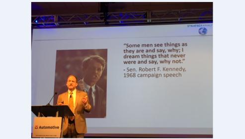
Keynoting the TU-Automotive event in Novi, Mich., last week on the 50th anniversary of the assassination of Senator Robert F. Kennedy I took the occasion to note the lofty visions to which Robert and his brother, President John F. Kennedy, aspired. We face our own challenges in the automotive industry today, with an annual global highway death toll of 1.25M. It is in the interest of mitigating that fatality rate that we pursue our own lofty objective of automating driving.

In my talk I cited President Kennedy’s sentiments, spoken at Rice University in 1962: “We choose to go to the Moon! We choose to go to the Moon in this decade and do the other things, not because they are easy, but because they are hard.”

There is no question that automating driving is hard. It is also expensive. As car makers look out over the range of changing vehicle ownership and usage behavior a red ocean of expensive, loss-producing opportunity emerges. From ride hailing to car sharing to electrification and autonomy, billions of dollars are being invested in startups, acquisitions and hiring sprees producing rivers of red ink.

At the same time, industry intruders from the tech community – most prominently Amazon, Apple, Alphabet and Alibaba (the A-Team) are circling ominously, licking their corporate chops at the opportunity to gobble up great chunks of the automotive and wider transportation industry. At stake are the hearts, minds and wallets of the driving and commuting public.

Of greatest concern to auto makers is the fact that this A-Team possesses the financial wherewithal to endure the flow of red ink and swim across the red ocean to achieve the objective: seizing control of the hard won customer relationships built upon more than 100 years of automobile manufacturing. The victory in this struggle may well be determined by something as simple as speech recognition in the form of the many digital assistants cropping up on mobile devices, in smart speakers and, now, coming to cars.

The A-Team made its first foray into customer ownership with smartphone integration in the form of the increasingly familiar CarPlay and Android Auto. Now Alexa, Google Voice, Siri, Cortana and others are coming to car dashboards. These systems have the ability to turn every car into a mobile search engine – with predictable results.

Standing in the path of these digital interlopers are Nuance Communications – with its hybrid natural language understanding technology – and a tiny startup called German Autolabs. German Autolabs is offering an over-the-top digital assistant – “Chris” – purpose built in cooperation with Nuance to serve the needs of drivers and passengers

Why is Chris so important? Because the A-Team has made it clear to auto makers that they won’t be segregating or shielding vehicle-based digital assistant users from broader customer aggregation activities. The drivers of cars who may use Alexa, Google Voice and the rest will be subject to the broader customer acquisition objectives of these external solution providers.

The A-Team is seeking to sell and service cars, if not actually manufacture them, and they want to manage vehicle ownership and usage behavior – a monetization opportunity ultimately representing trillions of dollars. If successful, car makers will be left swimming helplessly in their red ocean as the A-Team sails off into the sunset.

Only time will tell whether Chris can provide the critical differentiation and digital assistance infrastructure necessary to preserve auto industry customer relationships and connectivity. But without Chris, the traditional auto industry may be unable to swim across the red ocean rising around our ankles. The key to Kennedy’s vision, after all, wasn’t just getting TO the moon, it was also getting back FROM the moon.


The Best of IP at DAC 2018 Conference

The Best of IP at DAC 2018 Conference
by Eric Esteve on 06-15-2018 at 12:00 pm

Design IP is going well, with 12% YoY growth in 2017, even if the market is about $3.5B. But Design IP is serving a $400B semiconductor market. Can you imagine the future of the semi market if the chip makers couldn’t have access to Design IP? The same is true for EDA: it’s a niche market (CAE revenues was about $3B and IC Physical Design & Verification revenue was less than $2B in 2017) driving a $400B market!

We will concentrate on IP, as I am proudly part of the DAC IP Committee since 2016, and I would like to highlight some session during next DAC in San Francisco, including the two I am chairing.

I will certainly attend on Monday 25[SUP]th[/SUP] to this session “Minimizing IC Power Consumption with PPA Optimized IPs” chaired by Farzad Zarrinfar and moderated by John Blyler. Not only because Frederic Renoux, VP sales for Dolphin Integration will be one of the panelist (Dolphin is one of my rare customer to be located in France), with Lluis Paris from TSMC (another IPnest customer…), but because I strongly think that low power will be key in the near future. Let’s call it “Energy Efficiency” instead of just low power and look at the above picture: if SoC design stay as it is today, the total energy of computing will consume more than the world’s energy production in 2040!

We have been used to a communication only focused on SoC performance (like with Intel CPU, the only metric was x.y GHz), but the chip makers will have to invest into energy efficient chips development, as their customers (running data center or simply integrating IoT devices in their systems) will force them to provide better chips, energy efficient chips.

I will have no other choice than attending on Tuesday 26[SUP]th[/SUP] at 10:30 the invited session “IP and Architectures for CMOS Imager Sensors”, as I am the chairman! Moreover, I have suggested the topic to the Committee, as CIS is already a very healthy segment of the semi market, weighting $12B in 2017 according with YOLE. The CIS market has exploded to bring always more performant CMOS Imagerto the mobile phone industry where the camera is becoming the Top selling argument (you don’t sell a smartphone because it integrates the best Viterbi algorithm).

And the CIS market is expected to rebound, thanks to the automotive segment where mirrors will be replaced by camera (today) and when many cameras, radars, LIDAR will be integrated to support autonomous vehicle (tomorrow). I am sure that most of the readers don’t know about CIS architecture, and about the type of IP integrated into a CIS (just like me in January 2017 when I started to work on this technology). I can tell you, it’s fascinating! Plenty of innovation are needed, the designers play at the limits of physical science. You will certainly learn a lot and learn from the best WW experts like Jean-Luc Jaffard, CIS market veteran working for Prophesee , who will give a state of the art overview to introduce the topic.

Still on Tuesday 26[SUP]th[/SUP], at 1:30 pm, I will not miss this session “Has The Time For Embedded FPGA Come At Last?” chaired by Ty Garibay, the DAC IP Committee chairman, CTO of Arteris, after working Intel, Altera and TI! IPnest has released a report in April this year “eFPGA IP Market Survey & Forecast-2018-2028” showing that, if the industry confirms the adoption trend for embedded FPGA, this IP market should explode and pass the $1 billion in 10 years. The “usual suspects” are part of this session with presentation from Steve Mensor (Achronix), Cheng Wang (Flex Logix) presenting with John Teifel (Sandia National Laboratories) as eFPGA IP customer and Yoan Dupret (Menta). I say usual suspects as all of them are active in communication since a couple of years, including blogs in Semiwiki, with maybe a special mention to Flex Logix in term of marcom activity! Just a precision: to be selected to present in this session, one important criteria was to justify having a SoC customer, in production. All of them have at least one identified customer (and they can share the name).

There are plenty of other session I recommend attending, including “New Challenges for IP and VIP to Support Emerging Application or Algorithm” still on Tuesday 26[SUP]th[/SUP] , at 3:30 pm, that I am chairing too, with 6 submitted papers.

Or “Latest Developments in High Performance SoC Interface IP Standards” an invited session chaired by Chirag Dhruv (AMD), dealing with IPnest domain of expertise, Interface IP (see the market report and forecast on the above picture), but it’s difficult to name all the IP sessions. But I can guarantee that the quality of the papers, submitted or invited is excellent (foar having spent hours to review and select it)!

You should go on: DAC 2018 IP & Design and also select the topic which best fit your interest.

Eric Esteve from IPnest


Stanford and Semiconductors: A Unique Combination in the 1960s

Stanford and Semiconductors: A Unique Combination in the 1960s
by Daniel Nenni on 06-15-2018 at 7:00 am

This is the second in the series of “20 Questions with Wally Rhines”

At 8am on my first day of graduate school at Stanford, I joined the “Structure of Materials” class taught by Craig Barrett, the youngest faculty member in the Materials Science and Engineering Department. Craig had just returned from a post-doc in England and was energetically publishing papers, writing a book (along with Bill Nix and Alan Tetelman) and teaching classes. He passed out mimeographed copies (for a price) of the rough drafts of the book for the class text book. His distinguished undergraduate career in the same department led to a faculty appointment and his history at Stanford included a record in the high hurdles which still stood. Ultimately, his impatience with the academic world led to his departure to join Intel where he eventually became CEO (but that’s another story). Craig, as the youngest professor, also offered the benefit that he willingly joined the grad students at the “O” (short for Oasis) and purchased pitchers of beer when the graduate student money ran out (which was early in the evening).

There were lots of interesting people in engineering at Stanford at that time, since Frederick Terman, former Dean of Engineering had recruited a variety of rising stars in the semiconductor industry including William Shockley and Gerald Pearson, both of Bell Labs transistor fame. Shockley was more famous because of the Nobel Prize and, ultimately, more INFAMOUS as he redirected his research from semiconductors to racial differences in intelligence. Since he had the office next to ours, we kept a sign in the window labeled “Shockley’s Office is Next Door” just in case someone with a fire bomb lost direction or became confused. The McCullough Building was hardly a safe place anyway with research in II-VI and III-V semiconductors down the hall involving elemental materials that were poisonous in the parts per billion range. And T.J. Rodgers, who would in the future found Cypress Semiconductor, was running experiments in the basement with the first of Stanford’s ion implanters, causing unexpected and sometimes dangerous, results.

While I plodded my way through Craig’s course, my extracurricular life was stimulated by my residence in Crothers Memorial Dorm, fondly referred to as “Cro Mem”. It consisted of two buildings, side by side, one for graduate engineering and science majors and one for lawyers and MBA students. Although love was not great between the two buildings, there were frequent touch football games and mutual enjoyment of the promotional efforts of emerging wineries, like Wente Brothers and Inglenook, who provided free wine anytime we had a party, which was frequent. Judging from those I still know from Cro Mem, the wine promotion was very effective although maybe not for Wente and Inglenook. But parties required more than wine so we turned to the most innovative of the Cro Mem residents, Roger Melen. Roger arrived at Stanford with an undergraduate Electrical Engineering degree from, of all places, Chico State (Daniel Nenni: don’t take offense). He published a book titled “Understanding Operational Amplifiers” (which I didn’t) by his second year in graduate school and he was making money in a variety of entrepreneurial ways, like consulting for Bay Area electronics startups or writing articles for Popular Electronics. Whenever we needed money for a party, Roger generously wrote an article, received $400 and the party was on.


Image sensor made by Terry Walker, Roger Melen and Harry Garland

Meanwhile, Roger worked on his PhD thesis under Prof. Jim Meindl who had dozens of graduate students (many of whom came to make up the Who’s Who of the electronics industry) designing chips and producing them in the two-inch wafer fab on campus. Roger was working on the Optacon, a reading aid for the blind, developing an 8×16 pixel charge coupled device (CCD) for a compact version of the product. But Roger was much too innovative and productive to work only on his research. On the side, his consulting business had grown. He designed the electronics for all sorts of equipment that recent graduates were developing. Since most of these companies had very limited cash flow, Roger had to be content to accept future royalties in payment for some of his work. Over time, he discovered that these entrepreneurial customers, although skilled in engineering and product development, had lost the ability to count. Roger was concerned about being cheated on the royalties so he developed a system to overcome this deficiency. He performed the design work, as he always had, but instead of labeling the integrated circuits (IC’s) in the design, he and with his graduate student friend, Harry Garland, re-marked them with proprietary letters for one of the key IC’s in each design. He then assumed the supply chain fulfillment role by relabeling the IC’s and providing the parts for production.

Roger with fellow graduate student Harry created the name Cromemco, after the “Cro Mem” dorm, which in a few years became one of the very early, successful microprocessor based computers. They needed funding and publicity to start a company so Roger turned to his tried and true technique—writing articles for Popular Electronics but this time including the Cromemco name.

During this period, I completed my degree and headed to Texas Instruments where I was coincidentally assigned the task of developing CCD imagers. You can imagine our shock at TI when we saw a cover article of Popular Electronics entitled “Build Your Own Solid State Imager” by Roger Melen along with his graduate friends Terry Walker and Harry Garland. While Fairchild, Sony, RCA and TI competed fiercely to develop early CCD imagers, the graduate students at Stanford had beaten us to the punch. Or so we thought. The article provided circuit diagrams plus a block labeled “solid state imager”. To fill that block, the article instructed the reader to send a check or money order to Cromemco, which was actually just a student living in Crothers Memorial Dorm. For $25, Cromemco would provide the needed component. But instead of sending a CCD imager, Roger sent American Microsystems S4008-9 DRAM’s (this early DRAM did not automatically refresh the bits during readout and came in a ceramic package with a metal lid that could be replaced by a quartz lid) by popping the tops off the ceramic packages. The image quality was good enough for the hobbyists. Those $25 checks added up to over $50,000 and became critical seed money for Cromemco, which Roger and Harry sold in 1987.

20 Questions with Wally Rhines Series


2018 Semiconductor Forecasts Revised Up

2018 Semiconductor Forecasts Revised Up
by Bill Jewell on 06-14-2018 at 12:00 pm

Forecasts for 2018 semiconductor market growth have been revised upward from earlier in the year. In January to February 2018, projections ranged from 5.9% from Mike Cowan to our 12% at Semiconductor Intelligence. Forecasts released in March to June range from Gartner’s 11.8% to our 16%. The latest forecasts average an increase of 5.4 percentage points from the previous forecasts.


What has changed in the last few months? One factor is the first quarter 2018 semiconductor market was not as weak as expected. The first quarter is the seasonally weakest and is usually down from fourth quarter of the previous year. In the last five years, the first quarter has been down four times, three times declining 5% or more. 1Q 2018 declined only 2.4% from 4Q 2017.

The memory market accounted for most of the 21.6% semiconductor market growth in 2017. Memory grew 61.5% while the rest of the market grew 9.9%. The memory market remains healthy in 2018. The three major memory companies, (Samsung, SK Hynix and Micron Technology) all report a continued strong DRAM market. The three companies see some softening in the market for NAND Flash, but do not expect significant declines.

The major semiconductor companies are cautious in their revenue guidance for 2Q 2018. Guidance ranges from a decline of 1.2% from Qualcomm to an increase of 16% from MediaTek (bouncing back from a 17.8% decline in 1Q 2018). The high end of guidance ranges from Broadcom’s 2.2% to MediaTek’s 20%.


The overall outlook for key electronic equipment has not changed significantly from early in 2018 to recently. In January, Gartner projected the combined unit growth of PCs and Tablets in 2018 would be 0%. In April, Gartner revised the number up slightly to 0.5% – not a significant change. In December 2017, IDC expected smartphone units would increase 1.2% in 2018. In May, IDC revised it to a decline of 0.2%. Again, not very significant. The International Monetary Fund (IMF) has kept its projected 2018 GDP forecast at 3.9% growth, unchanged from January to April.


The increased optimism for the semiconductor market in 2018 can primarily be attributed to the memory market continuing strong, not weakening as many expected. There is still the possibility the memory market could collapse in the second half of 2018. However, we at Semiconductor Intelligence believe the most likely scenario is a softening of the memory market, not a collapse. Moderate quarter-to-quarter growth for 2Q 2018 to 4Q 2018 supports our 16% annual forecast.


Foundry Partnership Simplifies Design for Reliability

Foundry Partnership Simplifies Design for Reliability
by Bernard Murphy on 06-14-2018 at 7:00 am

This builds on a couple of topics I have covered for quite a while from an analysis point of view – integrity and reliability. The power distribution network and some other networks like clock trees are particularly susceptible to both IR-drop and electromigration (EM) problems. The first can lead to intermittent timing failures, the second to permanent damage to the circuit. There are a number of products to support analysis for power integrity and EM risks, but then what? You need to modify your design to mitigate those risks; the analysis tools won’t do that for you.

In both cases the fix is to reduce resistance in the relevant part of the network. Within a layer you can widen the interconnect but at points where the network crosses between layers, you need to add more vias (or via stacks) – more points of contact between layers → lower resistance → lower IR-drop and EM. But this is a very design, location and use-case-specific optimization not commonly found in implementation build tools, so implementation teams have often built their own Calibre-based applications to handle adding these vias.

Providing the ability to create your own apps is part of the value-add of the Calibre family, particularly through PERC (programmable electrical rule-check), which provides the infrastructure to scan the design to find named nets and where these cross between layers, flagging where vias must be added. The more sophisticated teams have probably also automated, to some level, adding those vias, perhaps through Calibre-YieldEnhancer.

But as always there’s a challenge. When processes were simpler, adding vias was relatively straightforward, but in advanced processes (e.g. 7nm) ensuring DRC and LVS correctness in changes becomes a lot more complex. Managing this complexity has become an iterative flow: automate via additions as well as you can, re-run DRC and LVS, then fix violations as required. Do-able but this can become very painful when you may need to implement changes at many nodes across large networks (such as in a power distribution network).

Of course a better way would be to make the edits correct by construction but that requires a very good understanding of the process and of course the tools. The Calibre team already has an app, PowerVia, to do this and have partnered with GLOBALFOUNDRIES to add rules in support of their GF7LP process (GF have plans to extend it to other processes), a capability which is now a part of their Manufacturing Analysis and Scoring (MASplus) and which they presented at the recent Mentor U2U user-group conference.

Analysis starts with target nets for enhancement – ports (like power and ground nets) and other user-selected nets. The flow uses PERC to identify nets not already labeled in the layout, along with where those nets cross layers, then YieldEnhancer/PowerVia adds DRC/LVS clean vias at those intersections to the extent they can be added (it will not remove existing user/tool-added vias). The GF flow adds as many vias as possible (consistent with not increasing area) at each of these intersections. I would guess the reasoning is that even if this might be overkill in some cases, when it comes to reliability overkill is not so bad.

How big a deal is this? GF showed benchmark info in which they boosted vias up to 120% over the starting point and the design was DRC/LVS clean, so no need for iteration. That’s a lot of vias if you had to add them manually, and still a lot of work if you had to iterate DRC/LVS following less than perfect fixes. The GF speaker (Nishant Shah) added a few more details in Q&A. The flow is GDS-based, so should be thought of today as a finishing step, not designed to take back (yet) to P&R. The app requires you to define which nets to address, though it will assume port nets by default. And the flow is designed primarily to address IR-drop and EM on high current-density nets. GF handles via-doubling for reliability in other nets in a different flow.

In discussion with Jeff Wilson (Director of Marketing for the DFM solution in Calibre) and Matt Hogan (PMM for Calibre design solutions), their enthusiasm for this type of solution – foundry-based apps on top of Calibre – was clear. They see design companies struggling to handle the workload added by these kinds of reliability enhancements. While they can script these solutions themselves using PERC and YieldEnhancer, the effort required from implementation and CAD teams – to develop and prove out scripts and to iterate to get to DRC/LVS clean – is becoming intolerable. A better solution is a foundry-sponsored app, building on the same platform, allowing for designer control on which nets to address, and then automating fixes correct by construction in one pass.

For more information on Calibre YieldEnhancer and Calibre PERC (where they handle a lot of other interesting checks – ESD, EOS, voltage-dependent DRC rules for multi-power/voltage domains and more), stop by Mentor’s DAC booth (#2621) June 25-28. You can view a full list of their booth and conference sessions HERE.


Looking Ahead: What is Next for IoT

Looking Ahead: What is Next for IoT
by Ahmed Banafa on 06-13-2018 at 12:00 pm

Over the past several years, the number of devices connected via Internet of Things (IoT) has grown exponentially, and it is expected that number will only continue to grow. By 2020, 50 billion connected devices are predicted to exist, thanks to the many new smart devices that have become standard tools for people and businesses to manage many of their daily tasks.

Smart connected devices boost customer’s engagement, increase visibility, and streamline communications, especially with new human-machine interfaces like Voice User Interface (VUI) the favorite interface for new digital assistants like HomePod, Alexa and Google Assistant for a good reason—80 percent of our daily communications is conducted via speech.

In the future, IoT will continue to advance at an extraordinarily rapid pace, with remarkable growth in many directions. The ultimate goal is to have a smart and completely secure IoT system, however many obstacles will need to be overcome before that goal can become a reality.

IoT and Blockchain convergence
The current centralized architecture of IoT is one of the main reasons for the vulnerability of IoT networks. With billions of devices connected and more to be added, IoT is a big target for cyber attacks, which makes security extremely important.

Blockchain offers new hope for IoT security for several reasons. First, blockchain is public, everyone participating in the network of nodes of the blockchain network can see the blocks and the transactions stored and approves them, although users can still have private keys to control transactions. Second, blockchain is decentralized, so there is no single authority that can approve the transactions eliminating Single Point of Failure (SPOF) weakness. Third and most importantly, it’s secure—the database can only be extended and previous records cannot be changed.

In the coming years manufactures will recognize the benefits of having blockchain technology embedded in all devices and compete for labels like “Blockchain Certified.”

IoT investments on the rise
IoT’s undisputable impact has and will continue to lure more startup venture capitalists towards highly innovative projects in hardware, software and services. Spending on IoT will hit 1.4 trillion dollars by 2021 according to the International Data Corporation (IDC).

IoT is one of the few markets that has the interest of the emerging as well as the traditional venture capitalists. The spread of smart devices and the increase dependency of customers to do many of their daily tasks using them, will add to the excitement of investing in IoT startups. Customers will be waiting for the next big innovation in IoT—such as smart mirrors that will analysis your face and call your doctor if you look sick, smart ATM machine that will incorporate smart security cameras, smart forks that will tell you how to eat and what to eat, and smart beds that will turn off the lights when everyone is sleeping.

Fog computing & IoT
Fog computing is a technology that distributed the load of processing and moved it closer to the edge of the network (sensors in case of IoT). The benefits of using fog computing are very attractive to IoT solution providers. Some of these benefits allow users minimize latency, conserve network bandwidth, operate reliably with quick decisions, collect and secure a wide range of data, and move data to the best place for processing with better analysis and insights of local data. Microsoft just announced a $5 billion investment in IoT, including fog/edge computing.

AI & IoT will work closely
AI will help IoT data analysis in the following areas: data preparation, data discovery, visualization of streaming data, time series accuracy of data, predictive and advance analytics,and real-time geospatial and location (logistical data). Here are a few examples.

Data Preparation: Defining pools of data and cleaning them, which will take us to concepts like Dark Data and Data Lakes.

Data Discovery: Finding useful data in defined pools of data.

Visualization of Streaming Data: On-the-fly dealing with streaming data by defining, discovering data, and visualizing it in smart ways to make it easy for the decision-making process to take place without delay.

Time Series Accuracy of Data: Keeping the level of confidence in data collected high with high accuracy and integrity of data

Predictive and Advance Analytics: Making decisions based on data collected, discovered and analyzed.

Real-Time Geospatial and Location (Logistical Data): Maintaining the flow of data smoothly and under control.

Standardization battle will continue
Standardization is one of the biggest challenges facing growth of IoT—it’s a battle among industry leaders who would like to dominate the market at an early stage. Digital assistant devices, including HomePod, Alexa, and Google Assistant, are the future hubs for the next phase of smart devices, and companies are trying to establish “their hubs” with consumers, to make it easier for them to keep adding devices with less struggle and no frustrations.

But what we have now is a case of fragmentation, without a strong push by organizations like IEEE or government regulations to have common standards for IoT devices.

One possible solution is to have a limited number of devices dominating the market, allowing customers to select one and stick to it for any additional connected devices, similar to the case of operating systems we have now have with Windows, Mac and Linux for example, where there are no cross-platform standards.

To understand the difficulty of standardization, we need to deal with all three categories in the standardization process: Platform, Connectivity, and Applications. In the case of platform, we deal with UX/UI and analytic tools, while connectivity deals with customer’s contact points with devices, and last, applications are the home of the applications which control, collect and analyze data.

All three categories are inter-related and we need them all, missing one will break that model and stall the standardization process.

IoT skills shortage
The need for more IoT skilled staff is rising, including a growing need for those with AI, big data analytics and blockchain skills.

Universities cannot keep up with the demand, so to deal with such shortage, companies have established internal training programs to build their own teams, upgrading the skills of their own engineering teams and training new talents. This trend will continue, representing an opportunity for new engineers and a challenge for companies.

Original article was published on R&D Magazine : https://www.rdmag.com/article/2018/05/looking-ahead-whats-next-iot

Ahmed Banafa Named No. 1 Top VoiceTo Follow in Tech by LinkedIn in 2016

Read more articles at IoT Trends by Ahmed Banafa


Mentor Emulation Platform Now available on Amazon Web Services

Mentor Emulation Platform Now available on Amazon Web Services
by Daniel Nenni on 06-13-2018 at 7:00 am

Emulation is a hotly contested EDA market segment (which is being won by Mentor) and EDA in the Cloud is a trending topic so putting the two together is a very big deal, absolutely.

The following is a quick email Q&A with Jean-Marie Brunet, Director of Marketing, Emulation Division, Mentor, a Siemens Business. If you have other questions for Jean-Marie let me know and I will get them answered. It has been an honor to work with the Mentor emulation team on our ebook and other topics and I can tell you from personal experience that they are consummate emulation professionals.

Mentor introduced Veloce Strato last year, and earlier this spring announced expanded footprint choices and configuration options. How does today’s news of Veloce as first hardware emulation available in the cloud fit into your larger strategy for this product line?
When we launched the Veloce Strato platform in 2017, we focused on customers’ current and future needs for greater capacity. Those needs for more capacity drive the Veloce roadmap to stay a step ahead of the size of designs our customers are building. We also began to communicate a strategy to deliver the best cost of ownership available. The Veloce StratoT family is about capacity scaling and options. So the announcement of Veloce on the Cloud is an extension to our strategy to add another option to our portfolio of offerings. Customers are asking for capacity on the cloud to be available. They really do not care what precise HW configuration is made available. They care about capacity, uptime, latency and use models. We will decide to put whatever Veloce HW is required to enable and grow the Veloce on the cloud business.

Why emulation on the cloud? What kind of demand do you see, and what about it do you think will be attractive to customers?
If we are able to put an emulator on the cloud, we can put pretty much anything on the cloud! We started with the emulator because logistically it is by far the most difficult piece of equipment to put on the cloud. The demand is currently limited to companies that do not have IT infrastructure access, so we are essentially at the early stages. The cloud-based access to Veloce capacity is eliminating a big barrier of entry related to infrastructure challenges. The attractive aspect is the scalable access to capacity on demand.

Why Amazon Web Services?
We started with AWS because of the scale of their deployment. Their Latency zone aspect was key to this enablement. The main thing to consider for an emulator to be on the cloud is that the design database should not be too far from the box, otherwise you are crippled by the latency challenge. Working in partnership with AWS we addressed this very efficiently.

Security is a major concern for any customer looking at cloud services, and this seems especially true with the sensitive nature of hardware emulation. What measures have you taken to address security?
It was our concern as well when we started this adventure over a year ago. We spent a considerable amount of time on this topic. I recommend that customers meet with AWS and look at the security measures they take. It is very impressive. Another way to look at this is by understanding what companies are already using AWS. Just the names of current AWS customers makes it obvious that security is handled seriously. And, as is always the case with security, everyone should do their own homework…

Is there anything specific or inherent to Veloce that makes it particularly amenable to a cloud use models?
Emulation on the cloud is all about virtualization. Using emulation in a virtual mode opens the door to the creation of many different emulator use models, or Apps, where each App targets very specific verification challenges. Apps are growing the emulation user community by simply bringing more challenges and the associated engineers to the list of tasks emulation can accomplish. This expanding user base for emulation, outside the traditional use model of simulation acceleration, means increased reliance on emulation resources. The Veloce emulator is the clear leader in virtualization use models so being on the cloud is a perfect fit for our technology.

Mentor Veloce hardware emulation platform now available on Amazon Web Services


ISO 26262 Traceability Requirements for Automotive Electronics Design

ISO 26262 Traceability Requirements for Automotive Electronics Design
by Daniel Payne on 06-12-2018 at 12:00 pm

Reading the many articles on SemiWiki and other publications we find experts talking about the automotive market, mostly because it’s in growth mode, has large volumes and vehicles consume more semiconductors every year. OK, that’s on the plus side, but what about functional safety for automotive electronics? Every time that an autonomous car has an accident or a fatality it makes front page news on CNN and across social media, so we’re keen to understand how safety is supposed to protect us from driving mishaps. The automotive industry has already published a functional safety standard known as ISO 26262, which is a necessary first step, and for us in the design community we need to be aware that this standard mandates traceability requirements.

An automotive system starts out in the conceptual phase with a set of written requirements, then as the system is refined into hardware, software and firmware we need to be able to trace and document how every requirement gets designed, implemented and tested. Because of time to market and complexity, there are no companies using a purely manual system for traceability of requirements, instead each team is using some form of software automation.

So the ISO 26262 standard covers the following range of activities which are part of a 10-part guildeline:

  • Conceptual phase
  • System level design
  • Design
  • Verification
  • Testing

Everything that a team does in these five activities must be traced back to a requirement. Here’s a snapshot of what the 10-part ISO 26262 guideline looks like:

Design Challenges
Some IC design teams can have hundreds of engineers assigned to a single project, and across such teams there is a variety of software being used, like:

  • Data management systems (Perforce) – tracking design files
  • Bug tracking (Bugzilla)
  • Verification plans and continuous integration (Jenkins)
  • Workspace management tools
  • IC point design tools (Cadence, Mentor, Synopsys, Ansys, etc.)

Semiconductor IP is purchased, re-used and created for teams designing an SoC, so this all has to be managed and tracked. Here’s a simplified work flow for IC design teams, and the large blue arrow pointing back to the left means that all this data needs to be traced back to requirements:

Modern IC designs can consume Terabytes of design, verification and test data across thousands to millions of files, which makes compliance with ISO 26262 traceability sound rather daunting. Having a software platform to manage all of this for us sounds ideal, a way to manage all of the data and IP blocks across my entire team and geographies. I’d call this IP Lifecycle Management (IPLM).

One commercial IP Lifecycle Management system out there is called Percipient, from Methodics, and I’ve blogged about them before over the past year or so. The Percipient tool is engineered to meet the needs of traceability requirements for the ISO 26262 standard, and here are some of the other industry tools it works well with:

Abstraction

With Percipient a design team can now connect high-level requirements to documentation to design to manufacturing, with traceability built-in. This methodology will keep track of all your semiconductor IP, cell libraries, scripts, verification files, results, bugs and even bug fixes. You use Percipient in all six phases of design to manufacturing:

The abstraction model used by Percipient enables it find and track all data from your SoC design project, it even knows low-level details like file permissions, bug tracking, locations for all IP instances, who is using each IP block, who owns an IP block, who created a cell, and even which workspace it all belongs to. Industry tools play well together with Percipient, by design. Here’s a quick summary of useful features in Percipient:

  • Workspace tracking
  • IP usage tracking
  • Release management
  • Bug tracking
  • IP versioning
  • Tracking design files
  • Tracking file permissions
  • Uses labels and custom fields
  • Handles hierarchy
  • Hooks for integrating any other tool

Self-documentation is a goal of the ISO 26262 standard and using a tool like Percipient really automates that process.

Summary
Driving a car today provides us mobility and we all want to arrive at our destination safely and without drama, so the automotive industry has wisely created and followed the ISO 266262 standard for functional safety requirements. The traceability part of the standard is now automated for semiconductor design through the use of a tool like Percipient. With it’s unique IP abstraction model this approach provides traceability across design, verification and testing.

The folks at Methodics will be attending the ISO 26262 To Semiconductors USA conference, June 11-14 in Michigan.

Read the complete White Paper here, after a brief registration process.

Related


Thermal and Reliability in Automotive

Thermal and Reliability in Automotive
by Bernard Murphy on 06-12-2018 at 7:00 am

Thermal considerations have always been a concern in electronic systems but to a large extent these could be relatively well partitioned from other concerns. Within a die you analyze for mean and peak temperatures and mitigate with package heat-sinks, options to de-rate the clock, or a variety of other methods. At the system level you might rely on passive cooling or plan for forced air or even liquid cooling. These methods treat heat as more or less a bulk property to be managed. But that approach alone is breaking down in a number of modern applications, for which automotive (in ADAS and autonomy) provides good examples.

What changed? Ambient temperatures in a car (up to 150[SUP]o[/SUP]C) are a lot more stressful than mobile devices have to consider. This isn’t new but we’re now packing those mobile technologies and more into the car, with much higher safety expectations. That’s just to start. Automakers need higher levels of integration of heterogenous technologies, in part driving a trend to advanced packaging where we now have to consider not only thermal effects within a die but also between stacked die. System builders also moving much more aggressively to advanced processes because they need the performance and lower standby power. But this means gates and wires crammed closer together with more heat concentrated in smaller areas. Worse yet, FinFETS with their wrap-around gates are unable to dissipate heat as effectively as traditional planar gates.

FinFETs have higher drive strengths, which is good for performance, but into narrower interconnects which increases the risk of electromigration (EM), impacting device reliability. Local heating also accelerates EM, and it increases power consumption and risk of timing failures. Heat can cause mechanical problems. In 3D stacks, or 2/5D on interposer, also on the board, heating can lead to warping between layers (Toyota had a recent problem with cracking solder joints caused by thermal stress). None of this is acceptable in automobile safety-critical functions.

OK, you get it. We need to analyze thermal more carefully, but there’s another challenge. In product design we like to split our analysis into different domains: timing, power, thermal, EM, die-level, package-level, board-level and system-level. It’s just too hard to do it any other way, right? We do detailed analysis in one domain at a time and we handle inter-dependencies between domains using margins. But increasingly the margin approach is requiring impractical over-design. More importantly, the automakers/Tier1s are demanding more cost-effective high-reliability solutions, which can only be accomplished though co-design and optimization from the system down to the die (incidentally this is also driving closer collaboration between the semis and the OEMs/Tier1s.) Effective thermal analysis has to span all of these domains, though here I’ll just touch on thermal analysis from system to die and related mechanical analysis.

Using ANSYS products, analysis spans a wide range of technologies, from RTL power analysis and RedHawk thermal, up to computational fluid dynamics (CFD) to model cooling at the system level, and ANSYS/Mechanical to model thermal-induced warping. Many of these are multi-physics analyses, pulling together fine-grained data from multiple domains (thermal, fluid modeling, mechanical, …) to provide accurate analytics for potential hotspots, rather than the approximations inherent in a domain-by-domain approach.

ANSYS starts with profiling at RTL, these days often driven through emulation-based modeling, so you might characterize for power profiles (developed in PowerArtist) during OS boot versus 4K streaming. From this they develop block power profiles and then chip profiles based on the floorplan. RedHawk CTA then builds a chip thermal model (CTM) containing understanding of hotspots in that die. In a multi-die package these analyses can be combined to provide a package-level thermal analysis, combined with a mechanical analysis of stress (and potential warping) in that configuration.

Up at the system level, thermal models for each of the components (chips, voltage regulators, sensors, …) are combined in an Icepak CFD analysis to assess steady state and transient thermal profiles, including whatever passive or active cooling may be provided. Naturally this analysis is iterative; you model system-level thermal profiles and take this back to the die for refined modeling. That gives you improved data on EM and other risks across the die, to which you can respond with appropriate design optimizations. Which in turn should provide a more accurate handle on thermal-related failure rates across the system. I don’t know if anyone in the automotive value chain is looking at this yet but based on what I’ve heard about rising expectations in ISO 26262, I wouldn’t be surprised to see this kind of analysis become a requirement at some point.

You can watch the recorded webinar (delivered by Karthik Srinivasan, Sr. Corporate AE Manager in the Semiconductor BU at ANSYS) HERE. He covers a lot more detail, including local thermal effects and doing power/thermal loop simulations using SIwave and Icepak at the system level. There is also some interesting discussion on where these methods are important beyond automotive. Well worth watching.


RAL, Lint and VHDL-2018

RAL, Lint and VHDL-2018
by Alex Tan on 06-11-2018 at 12:00 pm

Functional verification is a very effort intensive and heuristic process which aims at confirming that system functionalities are meeting the given specifications. While pushing cycle-time improvement on the back-end part of this process is closely tied to the compute-box selection (CPU speed, memory capacity, parallelism option), the front-end involves many painstaking setup preparation and coding. As such, any automation and incremental checks on the quality of work for both the design and the embedded codes used for its verification should help prevent unnecessary iterations and shorten the overall front-end setup time.

UVM Register Generator
Register Abstraction Layer (RAL) was part of the Universal Verification Methodology (UVM) supported features introduced in 2011. It provides a high-level abstraction for manipulating the content of registers in your design. All of the addresses and bit fields can get replaced with human readable names. RAL attempts to mirror the values of the design registers in the testbench, so one could use the register model to access those registers. A RAL model comprises fields grouped into registers, which along with memories can be grouped into blocks or eventually grouped into systems.

Aldec’s Riviera-PRO™ verification platform enables testbench productivity, reusability, and automation by combining the high-performance simulation engine, advanced debugging capabilities at different levels of abstraction. In its latest release (2018.02), it introduces RAL support.

As illustrated in figure 1a RAL model automatic generation involves taking the register specifications of a design (Riviera-PRO supports either IP-XACT or CSV spreadsheet formats) and generates the equivalent register model in System Verilog code.

To better appreciate how this register model is used in the UVM environment, consider how it interacts with the rest of components in the verification ecosystem as illustrated in figure 1b.

The creation of register model is normally followed by the creation of an adapter in the agent, which makes abstraction possible. It acts as a bridge between the model and the lower levels. Its function is to convert register model transactions to the lower level bus transactions and vice versa. The predictor
receives information from the monitor such that changes in values in the registers of the DUT are passed back to the register model.

As register model is captured at a higher level of abstraction, it does not require knowing either the targeted protocol or the register type to be accessed. Hence, from the testbench point of view, one can directly access the registers by name, without having to know where and what they are. Instead, the Register Model stores the details of all the registers, their types as well as their locations. It is the responsibility of the RAL to convert these abstracted accesses into read and write cycles at the appropriate addresses and using bus functional model. This convenient approach also makes tests to be more reusable.

Another component in the ecosystem is the sequencing part as shown in figure 1c. Sequences are built to house any register access method calls or Access Procedural Interface (API’s). Users may categorize these API’s into three types: active (read, write, mirror), passive (set, reset, get, predict) or indirect (peek, poke). The registers are referenced hierarchically in the body task to call write() and read(). The commands peek() and poke() which are utilized for individual field accesses.

Unit Linting
Linting is a prerequisite for good coding practice. It is common to have this done at the end of system code completion prior to checking-in the release. Unit linting which was previously done as stand-alone from Active-HDL Workspace, has been integrated as part of Riviera-PRO User Interface. Launching unit linting from this Riviera-PRO dashboard can be done through selecting a new button that will run unit linting on the open file and display the violations back on the console. This integration lets designer to work on a design, do the simulations as well as run linting from the same interface. It provides cross-probing facility that cross reference the violation versus the affected line of code as illustrated in figure 2.

Productivity Improvements and Partial Support to VHDL 2018
Code elaboration takes time as well as memory. In this Riviera-PRO release memory footprint during elaboration is reduced by as much as 80%, while improvement in simulation speed of 25% is noted for System Verilog constraint random design and up to 10x faster for assertion based designs with multi-clocks.

Proactive partial support is also available to the VHDL 2018 extension, which is going through the formalization process. This includes handling the conditional analysis directives and inferring constraints from initial values of signals and variables.

Furthermore, less restrictions were imposed on handling these constructs:
– Optional component keyword after the end keyword closing component declaration
– Denoting the end of the interface list with an optional semicolon sign.
– Allowing empty record declarations or qualified expressions or signatures of formal generic subprograms in a generic association list.

I had the chance to talk with Louie De Luna, Aldec Director of Marketing to further comment on these recent updates.

Would the corresponding System Verilog codes automatically generated for the register models and their associated adapters correct-by-construction or need to be validated?
We generate the UVM-RAL from user’s provided spreadsheet (*.csv). Successful generation is highly dependent on the input quality. Once generated, it is correct-by-construction. The users do not need to review it and they can easily attach it on their testbench.

Can designers skip those units already passed unit linting when they do full design linting?
Unit linting provides facility to conveniently perform code checks while it is being constructed. Unit linting may have simpler rules compares with the full linting that requires different ruleset. Designers have option to include or exclude particular checks. Linting is good, but since too many rules may clutter the process these filtering options should help.

What reference point used for performance comparison and any plan to extend beyond this supported list when VHDL 2018 ?
The comparison made for Riviera-PRO 2018.02 release is with respect to 2017.10. We plan to fully support when the VHDL 2018 is formally published.

For more detailed discussions on these features please check HERE