Earlier this Spring, Samsung Foundry held a technology forum, describing their process roadmap and supporting ecosystem developments (link). Recently, the larger Samsung Semiconductor organization conducted a Tech Day at their campus in San Jose, presenting (and demo-ing) a broader set of products. The focus of the day was on Samsung memory technology, encompassing non-volatile flash, DRAM, and GDDR roadmaps. The audience was more focused on system design and integration than silicon process technology, and the key Tech Day announcements reflected new Samsung memory products being introduced. (Samsung Foundry also made a major announcement.) Here are the highlights from the Samsung Tech Day.
Interesting Facts, Figures, and Quotes
In addition to the product introductions, there were some “sound bites” from the presentations that I thought were quite interesting:
- “EUV lithography for DRAM manufacture is currently in R&D, not yet in production – it will no doubt be introduced in future DRAM generations.” (a few layers)
- “Every 2 years, we create more data than we previously created in all of history.” (e.g., 160 ZB in 2025)
- “Facebook generates 4 PB/day alone.”
- “A future Class-5 fully-autonomous vehicle will generate 4TB/day.”
- “Analytics are changing the way in which professional sports are being played. The defensive strategies being employed against individual hitters have resulted in the lowest overall Major League Baseball batting average in 46 years.”
- “5G communications will be rolled out to 19 metropolitan areas in 2019.” (including San Francisco)
- “Data center corporations are aggressively adding a Corporate AI Officer (CAIO)executive position.”
- “Memory holds the key to AI.”
The focus of these examples was the requisite data capacity and bandwidth required of the current set of workloads. The key conclusion was:
“In the past few decades, computing evolved to a client-centric model. We are now moving to a memory-centric compute environment.”
One cautionary comment was provided:
“A significant percentage of the (unstructured) data being generated for analytics is ROT – redundant, obsolete, or trivial. A requirement for these memory-centric, data-driven applications will be to optimize the working dataset.”
Here are the major product announcements from the Samsung Tech Day.
256GB RDIMM
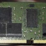
Samsung introduced the 16Gb DDR4 DRAM in 2017, utilizing their “1y nm” process technology. At the Tech Day, a 256GB “3D stacked” Registered DIMM stick was introduced. Although there’s been lots of attention given to 2.5D and 3D topologies for multiple (heterogeneous) logic die in a package, Samsung has been in production with stacked memory die for several generations – see the figure below.
Compared to an equivalent configuration with 2 x 128GB RDIMM, the 256GB RDIMM provides a ~25% power reduction, obviously a key factor in server design.
As the new RDIMM offers 2X the memory capacity in the same footprint, the maximum memory footprint of compute servers is likewise increased – e.g., 8TB in a 32-DIMM, 2P rack-mounted server. “In-memory” database transaction processing capabilities are expanded. For chip design, I was specifically thinking about the EDA applications for SoC electrical analysis, which are now able to accommodate 2X the model complexity, as well.
7LPP in Production
Although the theme of the Tech Day was the synergy between the Samsung Semiconductor product family and “memory-centric computing”, there was a major Samsung Foundry announcement, as well.
The “full EUV” 7LPP foundry process is now in full production, with comprehensive “SAFE” ecosystem support from EDA and IP partners.
Bob Stear, Senior Director, Samsung Foundry Marketing, indicated, “7LPP offers a 40% area reduction, and a 20% performance or 50% power improvement compared to 10nm. We are achieving a sustained exposure power output of 250W, enabling a throughput exceeding 1500 wafers per day. The utilization of single-exposure EUV lithography is truly a big leap in cost-effective production, compared to previous multipatterning-dominated process nodes. The number of masks is reduced by 20%.”
The figure above depicts the improved fidelity associated with (single-mask) EUV exposure versus (multi-patterned) 193nm ArF-immersion lithography.
Bob also hinted at future Samsung Foundry offerings, namely:
- (2nd generation) 18FD-SOI, w/embedded Magneto-resistive MRAM
- follow-on nodes 5LPE and 4LPE (E = “early” adopter), with PDK’s available in early 2019
- (more info to come at the next Samsung Foundry Forum in May’19)
- 3GAA (Gate-All Around) in 2019
“Smart” Solid-state Drive Architecture
A very unique announcement was the “Smart SSD”, a design that integrates an FPGA into the SSD package.
Xilinx collaborated with Samsung on the product engineering, offering a full application development and software library stack for the (Zynq, with ARM-Cortex core) FPGA integrated into the SSD.
The CEO of Xilinx participated in the product announcement, saying, “This new computational SSD architecture moves acceleration engines closer to the data, offering improved performance for database tasks and machine learning inference.”
Examples were provided of ~3X performance of (parallel-query) DB TPC-H transaction processing and ~3X business intelligence analytics (MOPS) throughput.
The Smart SSD architecture does present some interesting acceleration opportunities, and also some challenges. The endurance specifications for SSD’s vary significantly.
The system integrator utilizes the anticipated data communications workload profile to match the SSD endurance with the product requirements – e.g., an SSD “boot device” with limited activity (~0.1 – 1.0 effective drive writes per day, DWPD) to hard drive data caching (3++ DWPD). The use of an SSD in a new set of applications, such as providing accelerator engine data, requires new workload profiling and considerations for endurance reliability analysis (and over-provisioning) – a very interesting area for further research, to be sure. (The figure below provides an example of the SSD endurance calculations for Samsung SSD’s – a very interesting whitepaper is available here.)
Samsung Semiconductor definitely presented a unique perspective at their Tech Day, highlighting the need to focus on storage capacity and bandwidth for a new “memory-centric” computing environment.
-chipguy