The TSMC OIP Forum was very upbeat this year and now we know why. It wasn’t long ago that some media outlets and a competitor said 7nm would not be a popular node because it is too expensive blah blah blah. People inside the fabless semiconductor ecosystem however know otherwise. As I have said before, 7nm will be another strong node for TSMC, déjà vu of 28nm. The difference being that there will not be cloned 7nm processes like 28nm so TSMC market share and margins will remain strong, my opinion.
Let’s take a look at the Q3 2018 earnings call transcript and see what else we can learn:
Now let’s take a look at revenue by technology. 7-nanometer process technology contributed 11% of total wafer revenue in the third quarter. 10-nanometer accounted for 6%, while the combined revenue from the 16- and 20-nanometer accounted for 25%. Advanced technologies, defined as 28-nanometer and more advanced technologies, accounted for 61% of the total wafer revenue.
Apple is > 17% of Q3 revenue if you include 20nm (iPhone 6) and 16nm (iPhone 6+ and iPhone 7) legacy products.
Now let me make some comment about capacity and CapEx. At TSMC, we build our capacity according to the customer demand. We are continuing to increase 7-nanometer capacity to meet the strong customer demand. We reiterate our 2018 CapEx to be between US$10 billion and US$10.5 billion. In addition, as I have talked about before, although our leading edges capital cost continue to increase due to increasing process complexity, we are able to offset its impact to our CapEx by productivity improvements and further optimization of our capacity planning.
CAPEX can be further reduced by purchasing the equipment GF has in NY? TSMC will move from 5 layer EUV at 7N+ to 14 layer EUV at 5nm so they will need those extra ASML EUV Systems. TSMC will build new fabs for 5nm. In my opinion 5nm will be another big node for TSMC so I expect CAPEX spending to be at the high end for sure.
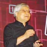
TSMC CEO C.C. Wei is a very strong leader and from what I am told he is loved by TSMC employees so I expect a very good run under his command. As we know from Intel’s latest debacle, a great CEO is key and C.C. is a great CEO, absolutely. He also has a sharp wit and is approachable and engaging which strengthens his credibility.
Now let me update you about the August 3 virus incident. On August 3, TSMC experienced a computer virus outbreak, which affected a number of computer systems and fab tools. The infection was due to misoperation and insufficient firewall controls. We have since corrected this problem to ensure such viruses will not happen again in the future. Our remediate actions including the following: implementing an automated system to guarantee fool proof execution so that such misoperation will not happen again; enhanced firewall control for fab isolation; and network control to each individual computer. More enhancements now are ongoing, too, for further improve tool immunity against future infections. TSMC sets top priority for such security enhancement.
From what I was told it was a vendor’s fault, but I am glad to see TSMC assume full responsibility and take the appropriate actions. I’m not a big fan of finger pointing as it is a sign of weak leadership.
Now let me talk about the N7 and N7+ and the EUV’s progress. TSMC’s N7 technology is now available for customers to unleash their innovations. This is the first time in the semiconductor industry the most advanced logic technology is available for all product innovations at the same time. We continue to work with many customers on N7, N7+ product design and expect to see more than 100 customer product tape-outs by end of 2019. We expect 7-nanometer to be a long node and will attract multiple waves of customer adoptions.
Absolutely.
N7+ is in risk production now. Since the N7+ has 15% to 20% better density and more than 10% lower power consumption, we are working with many customers for their second wave product designs in N7+. Although the number of tape-outs today account for a small portion of the total 7-nanometer tape-outs, we expect the activity to pick up at a rapid pace in 2020 and beyond. Because the N7+ is using a few layers of EUV photolithography to have better cycle time and patent control, we have made steady progress on EUV technology development towards high-volume production. Tool availability, EUV power, productivity, defect reduction, mask improvement, material and process optimization are all on schedule. A few customers have already made plans to adopt our N7+ in their 2019 products.
N7+ really is a test bed for EUV. They are doing 5 layers in preparation for a full EUV implementation of 14 layers at 5nm. It should not be hard to figure out the N7+ customers as they are the early adopters of 5nm. This half node approach has worked well since 20nm (Apple coming to TSMC) so I expect it to continue.
Let me move to our N5 status. Our N5 technology development is on schedule. We have completed the design solution development and are ready for customers’ design start. The N5 risk production schedule in first half 2019 stays the same. Compared to N7, TSMC’s N5 deliver 1.8x to 1.86x logic area reduction and close to 15% to 18% speed gain and ARM A72 core. We expect to receive first customer product tape-out in spring of 2019, followed by production ramp in first half 2020.
Apple will use 5nm in 2020 so you can bet it will be in HVM in the first half of 2020. From what I hear 5nm test chips are meeting/exceeding expectations and the PDK is solid so I see no reason to doubt TSMC’s 5nm schedule at this time.
Now let me talk about advanced packaging update. TSMC has been developing advanced wafer-level packaging technologies to integrated advanced SoCs, memories, integrated passive device, to enhance system performance. We believe our advanced packaging solutions will contribute to our business growth. We are now expanding the applications of both CoWoS and InFO especially for high-performance computing. Most of the CoWoS products require integration of SoC with High Bandwidth Memory, HBM, in 3D stack. We are making good progress in qualifying multiple HBM sources through close collaboration with customers and the DRAM suppliers. We are also working with a few leading customer on SoIC, which stands for system on integrated chips, where multiple heterogeneous chipsets will be integrated with close proximity to deliver better performance. And we target to start production in 2021 time frame.
TSMC has really done a nice job on packaging. I remember when CoWos came out there were quite a few doubters. Visionaries like myself and Herb Reiter saw this coming but even we are surprised at the amount of resources TSMC has committed to packaging and the excellent results. TSMC now has the MOST sticky foundry process in the world.
Now to the Q&A. Sometimes there are some very funny interactions but this is not one of them:
Michael Chou Deutsche Bank AG, Research Division – Semiconductor Analyst Is it fair to say that 7-nanometer sales portion will be more than 20% of total sales for the whole year next year?
Lora Ho Taiwan Semiconductor Manufacturing Company Limited – CFO and Senior VP of Finance Let me answer that. You have seen our report. The third quarter 7-nanometer accounts for 11%. The fourth quarter will be more than 20%. So for whole year 2018, 7-nanometer will contribute close to 10% of total TSMC revenue. Go beyond 7 — 2018, and we will have very, very strong ramp, in 2019 as well, we expect the revenue contribution will be much higher than 20%.
Randy Abrams Crédit Suisse AG, Research Division – MD and Head of Taiwan Research in the Equity Research Department Okay. The second question I wanted to ask was about the 7+ versus 5-nanometer. You mentioned 2020 would see the very strong ramp-up of tape-out and activity in volume on 7+. Is it your view — I think last conference, Mark said 5 was a little bit more conservative at this stage. So how’s your view now for interest activity and expectation for a steep ramp-up of 5 into 2020?
C. C. Wei Taiwan Semiconductor Manufacturing Company Limited – CEO & Vice Chairman We still expect very fast ramp on 5. The reason is simple. Because of a lot of products developed in the AI area, you need the speed, you need the lower power, and you also need a small footprint. So from this — from today, we can see when we work with our customers, the ramp will be steep again.
Roland Shu Citigroup Inc, Research Division – Director and Head of Regional Semiconductor Research Okay. Can you just reiterate the growth breakdown for this 4 platforms next year?
C. C. Wei Taiwan Semiconductor Manufacturing Company Limited – CEO & Vice Chairman Okay, let me give you some color on it. In the next few years, if we look at ahead, actually, the smartphone is going to be in our daily life even more and more. So we have a 4 growth engine: one is a mobile phone, actually it’s a high-end smartphone; second one is a high-performance computing; automotive; IoT. The mobile phone probably for TSMC will have a 5 year CAGR, if I look at it right from today, it will be mid-single digit growth. And the all others 3 platorms will have a very comfortably double-digit growth in the 5 year time frame.
Bill Lu UBS Investment Bank, Research Division – MD and Asia Semiconductors Analyst Great. I know 2018 is not over yet, but if you think about the next couple of years, I know TSMC has talked about a long-term growth rate of 5% to 10%. Now I feel like more recently, you’ve talked a lot more about the progress on 7-nanometers. We all know about Intel’s struggles with their process technology. And it’s public information. They’ve announced it, right? So — and then you’ve got some good design wins. Can you talk about your long-term outlook in 2019? Given these drivers you just said, out of the — 3 out of the 4 new drivers will be above 10%. So are we looking at something more towards the high end of that? Or how do you think about that?
C. C. Wei Taiwan Semiconductor Manufacturing Company Limited – CEO & Vice Chairman We continue to say 5% to 10% growth rate. Probably I would like to — following your question, I would like to say probably tends to be at the higher side of that 5% to 10%.
C. C. Wei Taiwan Semiconductor Manufacturing Company Limited – CEO & Vice Chairman Okay, actually the question is about the EUV and how much of the benefit we can get from the EUV, right? Usually, if we are not using the EUV, sometimes for the very critical dimension on the N7, you have to — or N7+, you have to use the 4 layers of lithography to pattern one of the critical dimension. Now using the EUV, you’re just using 1 layer so that you reduce the cycle time by 4x of photolithography, 4x of etch. Now you become 1 lithography, 1 etch. In total, how many layers we reduced? That depends on the customer’s requirement, but usually I just give you a hint already, right, 4 layer can become 1 and we are replacing some of the 3 layers to become 1 and we have a few layers of that. So that give you a hint. Cycle time reduction, definitely, because you do 4x into 1x, that’s a big advantage. Productivity-wise, today, EUV is progress very well — up to our expectation. And in fact, TSMC has turned on the 250-watt power and we believe we are the only one company continuously run the 250 watts EUV power so far today.
From what I hear ASML has 500-watt power working in the lab so 5nm EUV throughput should not be a problem. The question I have, now that EUV is in production, will ASML actually make money on EUV? After the many years of R&D and EUV broken promises? Billions of dollars must have been spent…
C. C. Wei Taiwan Semiconductor Manufacturing Company Limited – CEO & Vice Chairman Okay. Actually, I don’t want to comment on my competitors’ strategy. But let me, again, stress our mature nodes’ strategy. We continue to develop some of the specialty technology to meet the customers’ requirement, right, I just stated in that. And yes, a lot of specialty technology we are doing, I give you some example already, power management IC, CMOS, MEMS, everything. So that will help us to compete with our competitor. Actually, this kind of specialty technology particularly we have to work with the customer. And so that’s why I say working with the customer to meet their requirement. And that, in turn, to keep TSMC’s business. And that’s a way that we migrate the logic technology — pure logic technology to the more advanced node. But for the existing capacity, we develop into the specialty technology. And so our strategy is still meet customer’s requirement, but we don’t increase the existing logic capacity.
C. C. Wei Taiwan Semiconductor Manufacturing Company Limited – CEO & Vice Chairman I think the AI’s application would be everywhere, actually, from the edge server or to the end device that’s just like the smartphone of everybody. So this kind of a development is to our advantage because TSMC certainly have a technology leadership. In order the AI would be effective, you need a very advanced technology for the highest performance computing. So I don’t see the effect that you are talking about, this application is better than that so that affected the growth or something. No, it will be continues to grow. And I expect this growth much faster than I predicted here.
This is what I have been saying, AI everywhere. And with AI you get increased demand for performance, low power, and increased density which leads to increased leading edge process technology demand. This is really good news for TSMC and the fabless semiconductor ecosystem of course.
These are the questions that interested me. You can see the rest HERE. There is a lot more to discuss so let’s do that in the comments section.