webinar banner AI 2026 v2

UMC the Next China Chip Embargo?

UMC the Next China Chip Embargo?
by Robert Maire on 11-03-2018 at 7:00 am

The DOJ last week released a previously sealed indictment against UMC, Jinhua and three individuals for stealing Micron trade secrets. The indictment is very damning of UMC with very specific semiconductor technology files that were stolen by UMC related people then passed on to Jinhua through its joint development with UMC.

DOJ UMC indictment link

The indictment clearly lays out that UMC and individuals were responsible for the actual theft and that Jinhua was the recipient of the stolen goods. Usually the thief is treated more harshly than the receiver of stolen goods. The only thing that has likely kept UMC off the embargo list for now is that they are Taiwan based and are probably cooperating as fast as they can for fear of being put out of business.

To be clear Jinhua/China is far from innocent as UMC was just their henchmen.

UMC is clearly frightened as they have immediately severed all ties with Jinhua and tried to distance themselves. They canceled the DRAM joint development. Continuing the joint development would be pointless anyway now that Jinhua can’t get tools needed from the US to get a fab to work.

We would not be surprised if the stolen Micron information finds its way to other Chinese fabs such as Yangtze. That would likely result in an immediate embargo of the new receiver of stolen goods.

Its also obvious that if UMC gets embargoed that they would be forced out of business at some point as it would be difficult to keep their fleet of US made tools operating in their fab.

However we would not be surprised to see UMC get added to the embargo as it makes logical sense to punish the thief as well as the receiver. After the US initiates the embargo, there will likely be a quick settlement similar to ZTE where UMC will pay a huge fine and be forced to change out management just like ZTE did.

In the meantime, shipments to UMC will be halted just like shipments to ZTE were halted for several months. Just like in the ZTE case, US companies will be hurt as they won’t be able to do business with UMC, so it will be in the interests of the US to settle as well after US equipment companies scream.

Even though UMC is not a big spender it could be yet another down tick of overall Capex going into 2019. We think the embargo weapon could be used after the election when the fallout doesn’t matter, so we would stay tuned.

The stocks
This is obviously a very, very big potential negative for UMC. Its a positive for Micron, and a positive for TSMC. Its obviously a negative for semiconductor equipment companies in the US and ASML as well. We remained concerned as to what China’s response will be in the escalating tit for tat, and then how the US will respond in turn. We don’t think we have seen the last Asian company to be embargoed by the US, we expect more to follow.


Playing the Long Game with 56G SerDes

Playing the Long Game with 56G SerDes
by Daniel Nenni on 11-02-2018 at 12:00 pm

IP has always been a hot topic on SemiWiki with quite a bit of our readers doing the “make versus buy” analysis. SerDes is one of the more difficult “makes” so it is mostly a “buy” analysis made by networking class ASIC architects and a handful of other applications that demand high performance and throughput. Based on the recent traffic patterns, data centers and the coming 5G infrastructure are spiking SerDes interest, absolutely.

The new SerDes twist is “long reach”, a term I was not completely familiar with so I got on the phone with my goomba Mike Gianfagna at eSilicon. He put me in touch with Hugh Durdan, Vice President, Strategy and Products at eSilicon and Matt Burns, Technical Marketing Manager at Samtec Inc. Samtec is a privately held electronic interconnect solutions company that enables the SerDes “reach beyond the rack” implementation – high-speed serial communication over an eye-popping five meters of copper cable.

“eSilicon will demonstrate true long-reach capability for the most demanding system environments in next-generation 25 and 50 Tb/s switches with Samtec Twinax Flyoverä Cable Assemblies. Developers can accelerate their time to market with a high-performance, flexible, easy-to-configure SerDes that targets all of the common Ethernet, Fibre Channel and CPRI standards as well as proprietary rates common in data center and 5G
wireless infrastructure applications.”


5-meter prototype Samtec EBCM Series ExaMAX® Backplane Cable Assembly

Q: What’s different about the SerDes you are announcing?

A: from eSilicon. There are several things that set this device apart. It is a full DSP (transmit and receive) 56G SerDes in 7nm with true long-reach performance. Many other so-called DSP-based SerDes are in reality a hybrid with a digital transmit path but an analog receive path, which impacts performance. We also offer exceptional control and configurability through a graphical user interface that talks to the firmware running on an embedded SiFive processor built into the SerDes. From the GUI, users can access all monitoring features such as non-destructive eye diagrams, SNR & BER, bathtubs, histograms and power measurements.

Q: Regarding this “reach beyond the rack” demo, why is this significant?

A: from eSilicon. Customers want to leverage existing infrastructure and drive higher and higher data rates through legacy backplanes. With our ability to achieve low bit error rates over very long channels we enable customers to extend the life of their existing equipment vs. having to do a “fork-lift upgrade”. Data center customers also want extreme flexibility in connecting systems to each other. Thanks to the highly robust design of our SerDes and Samtec’s cable products, we are able to offer 56G operation over five meters of copper cable.

A: from Samtec. At 56G data rates, trace lengths on a PCB get really short. There are numerous design techniques engineers can use to combat this: advanced PCB laminates, additional PCB layers or clock and data recovery and retimers. Samtec’s solution is to get the signal out of the noisy and lossy PCB into low-noise, ultra-low-skew twinax copper cable as soon as possible. Long length copper cable also enables a paradigm shift in system architecture in the data center, whether inside the rack or beyond that rack.

Q: Tell me a little abou Samtec as my readers may not be familiar with your company. What do you make, where does it fit in the end product?

A: from Samtec. Samtec has been the service leader in the connector industry since our founding in 1976. At our core, we continuously support our legacy flexible stacking headers and sockets. Additionally, we are expanding our high-performance interconnect portfolio into backplane, board-to-board, precision RF, optical engines and high-speed cable assemblies based on our Twinax Flyover™ technology.

Q: Tell me about the long cables. What’s involved in manufacturing them? Why are they so accurate?

A: from Samtec. One key factor is our manufacturing process. Our twinax cables are co-extruded with low Dk FEP dielectric using real-time closed-loop control. This high-precision process eliminates the inconsistencies of individually extruded dielectric twinax cabling. Our cables are grounded via twinax copper alloy, eliminating the need for a drain wire. When combined with our high-performance connectors, the results are 56G data rates over the longest backplane cable assemblies in the industry.

The demonstration will be conducted in the Samtec booth #521 at Supercompute in Dallas from Nov. 12 – 15. Sign up now for a private briefing HERE. And Matt Burns has a nice blog series HERE.

AbouteSilicon
eSilicon provides complex FinFET ASICs, market-specific IP platforms and advanced 2.5D packaging solutions. Our ASIC-proven, differentiating IP includes highly configurable 7nm 56G/112G SerDes plus networking-optimized 16/14/7nm FinFET IP platforms featuring HBM2 PHY, TCAM, specialized memory compilers and I/O libraries. Our neuASIC™ platform provides AI-specific IP and a modular design methodology to create adaptable, highly efficient AI ASICs. eSilicon serves the high-bandwidth networking, high-performance computing, artificial intelligence (AI) and 5G infrastructure markets. www.esilicon.com

About Samtec
Much more than just another connector company, Samtec puts people first with a commitment to exceptional service, quality products, and convenient design tools. We believe that people matter, and taking care of our customers and our employees is paramount in how we approach our business. This belief is deeply ingrained throughout the organization, and means that you can expect exceptional service coupled with technologies that take the industry further faster. www.samtec.com


Basic Techniques for Managing EDA Business

Basic Techniques for Managing EDA Business
by Daniel Nenni on 11-02-2018 at 7:00 am

The “20 Questions with Wally Rhines” series finale

During the period from 1997, I had the privilege to work with Greg Hinckley, a superb “out of the box” thinker and excellent operational manager. We had such a common view of the world that we almost always agreed upon the best approach to problems and opportunities and hardly needed to confer, although we regularly did discuss almost all significant issues. One of our common attributes was a contrarian attitude. If everyone else was headed in the same direction, opportunity must lie in a different direction. That “Do what others aren’t doing” served as a guidepost for our moves at Mentor.

Following are some of the approaches that Greg or I brought to Mentor, or that evolved from combining our previous experience through interaction together

  • Listen for silence
    • Divisions, product groups, people and managers are always vying for the attention of top management and will usually let you know the good things they are doing
    • If you never hear from, or about, an entity in your organization, there are two possibilities:
      • They are doing nothing worthwhile and make no difference to the company, in which case they should be eliminated, or
      • They are trying to hide something, in which case they should be investigated


  • Life never gets any easier
    • Ignoring the problems of today only forces you to deal with bigger problems tomorrow
    • Never hope that excess inventory will be any easier to sell in the future than it is today—-write it off now
    • Never assume that an overdue account will find a way to pay you in the future—-it’s even less likely than the present


  • What you do infrequently, you do poorly
    • Send an annual invoice, not a quarterly one, for your customers to renew their maintenance contract — the person who deals with it will have to depend upon you to tell him how to handle it
    • Restrict the unfavorable options in your contracts so that customers only deal with them at renewal time. If they have to deal with options regularly, they will become very good at it.
    • Don’t expect your own organization to become efficient at things they rarely deal with—try to automate those things or consolidate them with someone who deals with similar issues regularly


  • Making rational decisions based upon data is more important than being right all the time
    • Can you provide a rational basis for why you are making the decision?
    • If you turn out to be wrong, you can retest your rationale and make a better decision next time
    • You may be wrong but at least you’re rational


  • Budgeting starts at the top
    • Asking organizations to determine how much they need to spend in the coming year (or quarter, month, day, etc.) is a worthless exercise and a waste of company resources—–the answer will almost always be more than the company can afford
    • Budgeting must start with an objective sales and revenue decision, heavily influenced by those who will have to achieve the sales. Budgets can then be developed that will fit into that sales and revenue plan.
    • Never be tempted to increase the revenue forecast when the cost budgeting pressures appear insurmountable. It will be even more difficult to reduce the budget later when the revenue comes in at (or below) the realistic level that is lower than the optimistic revised forecast.


  • In a chip company, management needs to focus first on what is NOT working. In a software company, management should focus first on what IS working.
    • Problems in a semiconductor company (low yields, rapidly falling prices, excess inventory, etc.) can bankrupt you quickly; fixing them has immediate, measurable benefit.
    • In a software company, inventory is unimportant and incremental revenue nearly equals incremental pre-tax profit. Costs are largely fixed because they are mostly people-related and people should not be treated as a variable expense. Incremental revenue is everything so maximum effort should be focused upon using existing resources to produce additional revenue.


  • Spend your time doing what others are NOT doing
    • Strategies that are similar to what the other mainstream companies are doing will rarely develop any unique advantage for your customers
    • Needs that are not being addressed offer more opportunity than those that are receiving lots of attention


  • For an employee, it is a great success for management to adopt your idea and claim it as its own, even if you are not acknowledged as the creator. For management, it is a great success to see employees act upon your idea and claim it as their own, even if they do not acknowledge you as the source.
  • In technical software, users rarely change the product they are using until it becomes incapable of completing the required task—not when it becomes, slow, inefficient, hard to use or unpopular.
    • Benchmarking with competitive products results primarily in price competition for the customer to secure a lower price to continue using the same software
    • Companies that offer a new and improved product would be better off to use their time by:
      • Participating in benchmarks of new applications that can’t be handled by the older, competitive tool, or
      • Finding new applications for the tool where there is not already an incumbent supplier.


  • When you acquire an EDA competitor, you don’t eliminate competition—-you create it. In EDA, people are the competitors and they keep doing what they are good at doing by creating new companies whenever the one they are working for is acquired.
  • A new product or service is not really profitable until you receive your first order from a customer with whom you’ve never interacted
    • As long as orders come only from direct effort and interaction by your own organization, you are expending too much money for the revenue you are achieving
    • When word of mouth and third party support start generating orders, you’ve gone viral and have a winning, profitable product


  • If you only play defense, your competitor will eventually score.
    • You must counterattack to make your competitor play defense
    • Selling your new, innovative products to your existing customers may be a starting point but success comes only when you penetrate new customers who are usually already served by your competitor
    • Statistically, your competitor will eventually get lucky if he keeps attacking your accounts and is not burdened with defense of his own accounts if you don’t attack them.


  • When your company is not number one is a specific market, always compare yourself to the leader(s). When, or if, you become number one, never compare yourself to anyone.
    • Market communication is all about consideration to purchase. You want to be considered when purchasing decisions are made so the association with the leader enhances the possibility of customer comparison of the leader’s product or service with yours.
    • If you are number one in a market, it’s counterproductive to provide your customer with a list of competitors to evaluate, even if you think your product is superior.


This is not meant to be a complete formula for successful EDA management. It’s a collection of ideas that aren’t normally discussed in business management training. Yet I believe that these observations, combined with other standard good management practices and an unwavering commitment to ethical treatment of customers, employees and shareholders, helped Mentor to recover from a difficult period and ultimately demonstrate leadership and success in a difficult high technology business.

The 20 Questions with Wally Rhines Series


Designing Integrated ADAS Domain Controller SoCs with ISO 26262 Certified IP

Designing Integrated ADAS Domain Controller SoCs with ISO 26262 Certified IP
by Camille Kokozaki on 11-01-2018 at 12:00 pm

As new automotive Advanced Driver Assistance System (ADAS) based product releases intensifies while a more stringent set of safety requirements are mandated, it is not surprising that subsystem and electronic suppliers are looking for pre-designed and ISO 26262 certified IP that can address both imperatives of schedule and safety when being integrated into SoCs. Add to that the necessity of lower power and higher performance, you begin to look at newer architectures that minimize footprint, risk, and effort and maximize the performance at the same time.

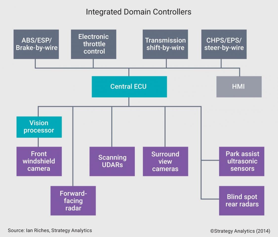
Traditionally, the electronic control units (ECUs) for individual ADAS applications have been placed throughout the car: the forward collision avoidance ECU located in the windshield, park assist ultrasonic sensors, and the processor in the rear. ECUs integrate the multiple ADAS applications into centralized domains to combine multiple ADAS functions. The new class of integrated domain controller ECUs utilizes data transferred from the car’s remote sensors such as cameras, LIDARs, radar, ultrasonic, and other sensors to the integrated domain controller for processing by a high-performance ADAS system-on-chip (SoC).

The IP in the integrated ADAS domain controller SoC must also meet the highest Automotive Safety Integrity Levels (ASILs), must be designed and tested for grade 1 and 2 temperatures, and must fully adhere to the automotive quality management process. In addition, to meet the power and performance requirements of the new integrated ADAS domain controller SoC architecture, designers are moving to more stringent process technologies, such as FinFETs, making it even more important to use automotive-certified IP in advanced foundry processes.

A Shift to Integrated ADAS Domain Controller SoC Architectures

According to the August 2016 Traffic Safety Facts Research Noteby the National Highway Traffic Safety Administration (NHTSA), “the nation lost 35,092 people in crashes on U.S. roadways during 2015, a 7.2% increase which is the largest increase in nearly 50 years.” It was analyzed that about 94% of those accidents were caused by human error, and the rest by the environment and mechanical failures.

The opportunity to reduce car accidents is making automotive ADAS even more critical. Automatic emergency braking, pedestrian detection, surround view, park assist, driver drowsiness detection, and gaze detection are among the many ADAS applications that assist drivers with safety-critical functionalities to reduce car accidents. Figure 1 shows an integrated ADAS domain controller SoC with a centralized ECU where data from numerous sensors travels to a central ECU and is then processed via an ADAS processor.


Figure 1: Data from sensors travel to a central ECU and are processed via a vision processor

High volumes of data are driving the adoption of 64-bit processors for automotive ADAS applications. The shift from a distributed architecture to a more centralized ECU is more prevalent, and since the ECUs are integrated, the ADAS SoCs are becoming very complex, requiring the latest semiconductor features, semiconductor process technologies, along with other technologies for ADAS domain controller SoCs:

  • Ethernet manages high data volume including time-sensitive data and reduces point-to-point wiring
  • LPDDR4/4x operates at data rates of up to 3200 megabits per second and beyond, which speeds up the DRAM operations in automotive-grade SoCs
  • MIPI standards like MIPI Camera Serial Interface and Display Serial Interface provide high-performance connectivity in imaging and display applications
  • PCI Express has high-reliability processor-to-processor connectivity for 4G radios or the future 5G radios and external SSDs
  • 5G and IEEE standards, like 802.11p, help provide real-time updates of maps or images to and from the Cloud, and vehicle-to-vehicle or vehicle-to-infrastructure communications
  • Security protocols in hardware and software for data protection to and from connectivity via USB, WiFi or Bluetooth
  • Sensor and control subsystems offload the host processor and fuse sensor data to manage the different type of sensor data provided by the sensors
  • More advanced manufacturing process technologies from the traditional 90-nanometer (nm), 65-nm and 40-nm to more advanced 16-nm, 14-nm, and even 7-nm FinFET processes

Safety-critical applications are significantly increasing the adoption of ADAS SoCs. However, it is required that the ADAS SoC along with all semiconductor components including the IP that is integrated into the SoC meet the ISO 26262 functional safety standard.

Meeting ISO 26262 Functional Safety Standard Requirements

ISO 26262 is a standard that defines the impacts of failures in automotive systems at four different Automotive Safety Integrity Levels (ASILs): A, B, C, and D; ASIL D is the highest level of functional safety. The ISO 26262 standard defines all the processes, development efforts, and standards that automotive development organizations must implement and comply with when developing products for safety-critical systems. A key objective of ISO 26262 standard is to minimize the susceptibility to all types of random hardware failures, including permanent failures or transient failures, by:

  • Defining the functional safety requirements when developing products
  • Applying rigor to the development process
  • Defining a safety culture
  • Implementing safety features to minimize the impact of hardware failures
  • Assessing and analyzing the impact of safety features to ensure mitigation of hardware failures

Industry-accredited inspection companies, such as SGS-TUV Saar, are available to audit products and processes for compliance and certification of ISO 26262.
The ISO 26262 certification process includes multiple steps, policies, and reports and must start from the very beginning of product development. For example, the Failure Mode Effect and Diagnosis Analysis (FMEDA), a report that development teams generate, provides all the information regarding the adherence to ISO 26262 from a functional safety perspective.

Created by design and verification engineers, the report is a critical component of an ASIL assessment, not just for evidence of compliance but also for design targets and a rating assessment at the end of the development flow. Designated safety managers, separately from the development organization, who are fully trained to monitor the development process, milestones and product reviews, ensure all the documentation and traceability is completed throughout the SoC development flow as defined by the standard.

The FMEDA report also includes a summary of the safety features, their development, and verification. It clearly documents the safety features contained in the products and how these products react to the random faults that are injected into them. The FMEDA report is mandatory and is given to all parties involved in the product review process.

How ISO 26262 Certification is Implemented

A standard SoC or IP product development flow starts with register-transfer level (RTL) design, which is then implemented, verified, and validated in hardware and software in the final prototypes. An ISO 26262 compliant development adds additional steps over the standard design process including at the very start when defining a core architecture and specification. Designers define a safety plan that includes safety features and goals. The product team and safety manager review the safety plan and strategy to achieve the designated functional safety for the end application.

It is important to conduct a failure analysis by injecting faults to assess the safety level and the system’s reaction to those faults. The FMEDA shows a fault injection analysis for both permanent and transient faults to assess the impact. The analysis and assessments are clearly documented in the FMEDA report as part of the ISO 26262 certification process along with the safety manuals. This entire process is shown in Figure 2.

Figure 2: An example of a standard SoC or IP design with additional ISO 26262 certification steps and requirements

The safety manual in the ISO 26262 certification process defines the safety features in the product, which is critical to the operation of the product. The standard provides some guidelines as to the effectiveness of safety features that can detect possible failures. Safety features for IP product design fall into three categories: protection mechanisms, replication, and various.

  • Protection mechanisms, such as protecting the interface between the IP in the SoC architecture with the protection of elastic buffers, parity protection on the data path and configuration registers, and error correction code protection for both writes and reads.
  • Replication is a safety feature category that includes duplicating (or triplicating) key modules and using voting logic to ensure redundancy.
  • Various includes parity checks for all the state registers, single cycle pulse validity, various dedicated interrupts, and hot state machine protection for bad states.

The process to meet ISO 26262 functional safety certification is stringent from creating the FMEDA report, designating a safety plan that defines safety features for the target ASIL, to employing a safety manager and documenting and reviewing every milestone with all the stakeholders. In addition to meeting ISO 26262 functional safety requirements, integrated ADAS domain controller SoC development teams and the rest of the supply chain, including the design IP provider, must adhere to automotive reliability and quality requirements.

To meet the automotive reliability standard as defined by the automotive industry, automotive SoCs and IP must be designed and tested to meet very low defect densities which are measured by Defects Parts Per Million (DPPM). The automotive industry has a requirement for less than one DPPM, encouraging designers to set a goal of zero defects per million throughout the automotive product lifetime of 15 years.

Meeting temperature grade is another reliability requirement. For ADAS, the highest level of operating temperature is Grade 1 which requires up to 125 degrees Celsius ambient or 150 degrees Celsius junction temperatures. Each company within the automotive supply chain has a proprietary temperature mission profile to which they design and test their products. SoC and IP designers who are developing products for the different ADAS applications take the temperature mission profiles into account during the development process. Different requirements such as electromigration, transistor aging, and transistor self-heating must be considered against the temperature mission profile for the different devices.

Synopsys offers a portfolio of automotive-certified IP that is ASIL Ready ISO 26262 certified, designed, tested for grade 1 and 2 temperatures, and fully adhere to the automotive quality management process. For information view the DesignWare IP for automotive SoC web page.Based on a technical bulletin posting By Ron DiGiuseppe, Automotivie Segment Marketing Manager, Synopsys


Wi-Fi Standards Simplified

Wi-Fi Standards Simplified
by Bernard Murphy on 11-01-2018 at 7:00 am

In the world of communications, the industry fairly quickly got a handle on a naming convention for cellular technology generations that us non-communication geeks could understand – 2G, 3G, 4G and now 5G, (though some of us could never quite understand the difference between 4G and LTE, at least as those terms are widely and no doubt inexpertly used). This is a nice steady progression, easy for us uncultured masses to remember, with no confusing affixes.

Bluetooth has from the beginning followed a largely similar convention in generation naming from 1.0 up to current BT 5 which drops the ”.0” on the name, not coincidentally aligning numerically with the latest cellular standard. There is a sub-generation of 4.0 (at least initially), known widely as BLE (Bluetooth Low Energy) but we generally understand that this is a low-energy variant on the underlying standard.

Wi-Fi on the other hand soldiered on in geekdom, oblivious to the needs of the masses, by sticking a bewildering array of postfixes on the root 802.11 standard name. I guarantee that no-one in the general public would have any idea what you were talking about if you asked them about say 802.11n, whereas many would profess at least some familiarity with 5G, if with the name only. The Wi-Fi Alliance recognized this wasn’t great for marketing and has recently switched to a much easier naming convention, at least for the most recent generations.

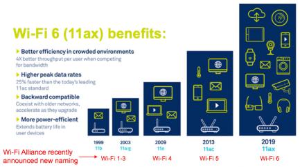
For the newer generations of the standard, 802.11n becomes Wi-Fi 4, 802.11ac becomes Wi-Fi 5 and 802.11ax becomes Wi-Fi 6. For 802.11a/b/g I hear differing stories. Fortune magazine says that these names won’t change. Another contact says (plausibly) that these will be known as Wi-Fi generations 1, 2 and 3. Now isn’t that easier to understand? You may not know what they are but all of us can understand that as you progress from Wi-Fi 1 to Wi-Fi 6, you get better technology at each stage, for which you are prepared to shell out more money (see, that’s marketing).

We’re a bit more sophisticated than that, so what are 4-6? Wi-Fi 4 (aka the “n” version) supports transmission rates 5-6 times faster than the Wi-Fi 3 version, higher reliability and supports MIMO (multi-input, multi-output) where multiple antennae at receiver and/or transmitter further boost reliability and transmission rates.

Wi-Fi 5 (aka the “ac” version), introduced in 2014, increases rates by a factor 2 or more and more efficiently uses bandwidth so more users can be served at speed in one network. However, more efficient usage is only in the downlink. So you can all watch cat videos with minimal buffering but the network bogs down if you all want to share with friends. Wi-Fi 6 (aka the “ax” version), expected to be ratified by the end of 2019, goes one step further, packing multiple users more effectively in both downlink and uplink, serving an expected 4X improvement in throughput in high user density environments (think of a stadium). It also offers a 25% improvement in peak data rate.

So Wi-Fi generation naming is now understandable and mostly aligned with cellular and Bluetooth naming. There’s an apparent disconnect in that the latest Wi-Fi is Wi-Fi 6, whereas cellular is at 5G and Bluetooth is at BT5. But the official Wi-Fi 6 is a year away so perhaps numeric synchronization isn’t too far off. When we’re checking out phones or other devices, we should reasonably soon be able to look for all communications to be at level “N” (maybe 6?) no matter what the underlying technology. That will make life a lot simpler, certainly for me.

I have to thank Franz Dugand, Sales and Mktg Director for Connectivity at CEVA for these insights. Naturally CEVA has a wide range of Wi-Fi IPs across these standards, including Wi-Fi 6, ranging from low-power to high-performance to multi-gig rates. CEVA have been in the Wi-Fi core licensing business since 2002 so they’re very well known and established in the space. You can learn more about their RivieraWaves Wi-Fi platforms HERE.


Architecture for Machine Learning Applications at the Edge

Architecture for Machine Learning Applications at the Edge
by Tom Dillinger on 10-31-2018 at 2:01 pm

Machine learning applications in data centers (or “the cloud”) have pervasively changed our environment. Advances in speech recognition and natural language understanding have enabled personal assistants to augment our daily lifestyle. Image classification and object recognition techniques enrich our social media experience, and offer significant enhancements in medical diagnosis and treatment. These applications are typically based upon a deep neural network (DNN) architecture. DNN technology has been evolving since the origins of artificial intelligence as a field of computer science research, but has only taken off recently due to the improved computational throughput, optimized silicon hardware, and available software development kits (and significant financial investment, as well).

Although datacenter-based ML applications will no doubt continue to grow, an increasing focus is being applied to ML architectures optimized for “edge” devices. There are stringent requirements for ML at the edge – e.g., real-time throughput, power efficiency, and cost are critical constraints.

I recently spoke with Geoff Tate, CEO at Flex Logix Technologies, for his insights on ML opportunities at the edge, and specifically, a new product emphasis that FlexLogix is undertaking. First, a quick background on DNN’s.

Background

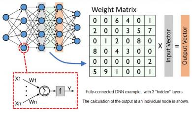
A “deep” neural network consists of multiple “layers” of nodes. At each node, a vector set of inputs is provided to a computational engine. The output of each node is further refined by a (potentially non-linear) activation function calculation, which is then forwarded to the nodes in the next layer. The final layer provides the DNN decision from the original input set – i.e., a “classification” result of an input image to a reference set of objects.

Figure 1. Illustration of a simple DNN, with 3 “hidden layers”. The computation at each layer is a matrix multiplication of the input vector and a matrix of weights.

Numerous DNN topologies are used in practice – the figure above depicts a simple, fully-connected multi-layer 2D design. (More complex “3D” topologies and implementations with feedback connections in the hidden layers are often used, which are optimal for specific types of inputs.)

Each node in the DNN above performs several computations, as shown in the figure below. At each node in the layer, a set of weights are multiplied against the input value, then summed – i.e., a “multiply-accumulate” (MAC) calculation. An (optional) bias value may be incorporated into the sum at each node. The MAC output is input to a normalizing “activation” function, which may also incorporate specific parameter values – activation function examples are illustrated below.

Figure 2. Expanded detail of the calculation at each node in a layer, and some examples of activation functions.

During the DNN training phase, a reference set of inputs is applied. The selection of the initial weights, biases, and activation parameters at each node is an active area of research, to optimize the training time. (The simplest method would be to pick values at random from a normalized distribution.) The input reference set proceeds throughforward evaluation and the DNN result compared to the expected output.

An error difference is calculated at the output layer. A backwards optimization phase is then performed, evaluating an error gradient dependence for the network parameters. Internal DNN values are then adjusted, and another forward evaluation pass performed. This training optimization iterates until the DNN classification results demonstrate acceptable accuracy on the input reference set.

The DNN values from training are subsequently used as part of the production inference engine, to which user data is now the input.

DNN in the Data Center

The initial DNN (training and inference) implementations in the datacenter utilized traditional von Neumann CPU and (DRAM) memory resources to perform the MAC and activation calculations. The DRAM bandwidth to the CPU core is typically the throughput bottleneck.

A transition to GPU-based cores for DNN calculation was then pursued, to leverage the SIMD dot product MAC calculations prevalent in GPU image processing. GPU’s have a drastically different architecture, with very wide internal vector datapaths – e.g., ~1024 bits wide. As a result, to improve core resource efficiency, a “batch” of inputs is evaluated concurrently – e.g., 32b floating-point DNN parameter values could be concatenated into a wide vector to evaluate a batch size of 32 inputs in parallel through the DNN layers. Yet, the local memory associated with each GPU core is relatively small (KB’s). Again, the (GDDR) memory bandwidth is a DNN performance-limiting factor.

New chip architectures are being aggressively pursued for ML applications – e.g., Google’s Tensor Processing Unit (TPU). And, due to the intense interest in the growing base of ML applications, numerous chip start-ups have recently received (initial round) VC funding – see the figure below.

Figure 3. Examples of ML hardware startups (from [1]).

Additionally, cloud service providers are deploying FPGA hardware to offer effective, easily-reconfigurable DNN capabilities. [2]

DNN’s using conventional CPU and GPU hardware architectures are throttled by the access bandwidth to retrieve the weights and biases for each layer evaluation. Training presents an additional data constraint as these parameter values are required to compute both the forward evaluation and the backward optimization error gradients, as well. As an example, the ResNet-50 DNN is commonly used as a reference benchmark for image classification, a complex (3D) 50-layer convolutional network topology. A forward pass evaluation utilizes ~26M weights. [3] Depending upon the data precision of these parameters, the memory bandwidth required to access these values for use in a layer computation is very high.

ML Applications at the Edge

My conversation with Geoff at Flex Logix was very enlightening. First, he shared some of the characteristics of edge applications.

“An ML application will typically pursue DNN training at the datacenter, and then transfer the DNN parameters to edge hardware for inference.”

“Often, a DNN hardware implementation quotes a peak throughput, in trillions of operations per second (TOPS), and a related power efficiency (TOPS/W). Yet, it is important to analyze what memory bandwidth and batch evaluation assumptions are used to calculate that throughput.”

“Edge customers will typically be utilizing (sensor) input data corresponding to ‘batch_size = 1’. Maybe a batch size of 2 or 4 is applicable, say if there are multiple cameras providing video frames per second input. The datacenter architectures that merge parallel input sets into large batch size DNN evaluations to optimize MAC efficiency just don’t apply at the inference edge.”

“High batch count increases overall classification latency, as well, as the parallel input set is being merged – that’s of little consequence for typical datacenter applications, but additional latency is not appropriate at the edge.”

I asked Geoff, “How is Flex Logix approaching this opportunity at the edge? What elements of the existing embedded FPGA technology are applicable?”

Geoff replied, “We have announced a new product initiative, NMAX. This architecture builds upon many of the existing features of our embedded FPGA, specifically:

  • a tile-based building block that is readily arrayed into an (m X n) configuration
  • a combination of logic LUT cell and MAC engines in a DSP-centric tile
  • a method for optimal embedding of SRAM macros of varying size between tiles (link)
  • a rich set of external connectivity options when embedded within an SoC design

A block diagram of a single “NMAX512” tile is illustrated below.

Figure 4. An architectural block diagram of the NMAX512 DNN tile, and an array of tiles depicting the L2-level SRAM between tiles.

Each tile contains 8 NMAX clusters. Each cluster contains 64 MAC’s using an 8b x 8b parameter data width (with options for 16b x 16b), with a 32b accumulate. There is a total of 512 MAC’s per tile. The programmable EFLX logic LUT’s perform the activation functions for the DNN layer. The weight and bias values for the layer are accessed from the local (L1) SRAM within the tile.

An embedded (L2) SRAM between tiles stores the intermediate DNN results and parameter values for successive layer calculations. New values are loaded into the L2 SRAM in the background during forward evaluation. The required data bandwidth for system DRAM memory is reduced significantly.

Geoff added, “The time to reconfigure the NMAX tile with new DNN layer with new DLL layer data (from L2) is very fast, on the order of 100’s of nsec.”

“How is the NMAX tile implementation for a DNN developed?”, I inquired.

Geoff answered,“ML developers utilize the familiar TensorFlow or Caffe languages to define their DNN topology. We will be releasing a new NMAX implementation flow. Users provide their TF or Caffe model, and the NMAX compiler fully maps the data and logic operations to the MAC clusters and reconfigurable EFLX LUT logic. All the sequencing of DNN layer evaluation is mapped automatically. The physical LUT placement and logic switch routing configuration is also automatic, as with a conventional embedded FPGA.”

Geoff continued, “Our preliminary performance models indicate we will be able to achieve ~1GHz clocking (TSMC 16FFC), or roughly ~1 TOPS throughput per tile(with LPDDR4 DRAM, L2 SRAM size optimized for the DNN). The distributed L2 SRAM helps maintain a very high MAC and activation function utilization.”

“Speaking of performance modeling, do you have NMAX benchmark data?”, I wondered.

Geoff replied, “We prepared the following data for NMAX compared to other architectures, such as the Nvidia Tesla T4, for the ResNet-50 DNN benchmark with Int8 parameters. Note that the NMAX architecture enables a wide span of tiled array sizes, with corresponding throughput scaling for the batch_size = (1, 2, 4) of greatest interest to edge customers. The initial MAC utilization and total power dissipation is much improved over other architectures, as well.”

Finally, I asked, “What is the NMAX deployment schedule?”

Geoff answered, “We are starting to engage partners now, in terms of potential NMAX sizes of interest. Our engineering team will be finalizing IP area/performance/power specs in 1H2019, as well as finalizing the NMAX compiler. A tapeout release with a specific tile and SRAM configuration will occur in 2H2019, to provide evaluation boards to customers.”

There is clearly a lot of activity (and VC investment) pursuing optimized DNN hardware architectures for datacenter applications. There is certainly also a large market for (embedded IP or discrete) hardware focused on the power/perf/cost constraints of the low batch-size ML applications at the edge. Flex Logix is leveraging their expertise in reconfigurable (DSP plus logic) functionality in pursuit of this opportunity.

It will be an interesting R&D area to follow, for sure.

-chipguy

References

[1]https://origin-blog.appliedmaterials.com/vc-opportunities-ai-developer-ecosystem

[2]Putnam, A., “The Configurable Cloud — Accelerating Hyperscale Datacenter Services with FPGA’s”,2017 IEEE 33rd International Conference on Data Engineering (ICDE),https://ieeexplore.ieee.org/document/7930129/ .

[3]https://www.graphcore.ai/posts/why-is-so-much-memory-needed-for-deep-neural-networks


Mentor’s Busy ITC and Major Test Product Updates

Mentor’s Busy ITC and Major Test Product Updates
by Tom Simon on 10-31-2018 at 1:00 pm

In conjunction with the 2018 International Test Conference, Mentor has several interesting test announcements. They also have a busy round of technical activities, including a number of technical papers, presentations, tutorials and a poster from a major customer about using Mentor. I’d like to touch on the two product related announcements, because they are pretty interesting.

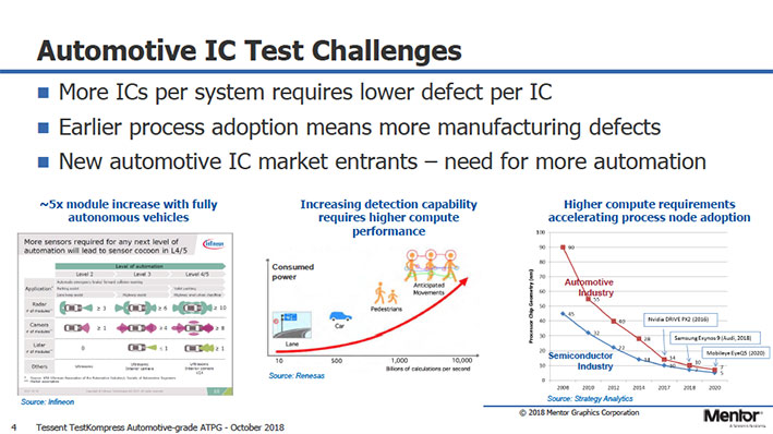
There is probably no area other than automotive where reliability has received more focus lately. First off, zero defects are a prerequisite for ISO 26262. Also, the automotive semiconductor market is experiencing higher growth rates than almost any other sector. As such, automotive applications have become the reference for quality and reliability. It is pushing the development of improved methodologies and is setting the standard for the highest reliability.

Automotive is on a steep complexity growth curve, both historically and for the immediate future. It used to be that automotive semiconductors could leisurely stay behind the bleeding edge of technology. However, ADAS and new requirements for infotainment have brought automotive computing and data transfer requirements to the point where only the most advanced nodes will suffice. Going from Level 2 to Level 4/5 for ADAS will increase the number of sensor modules by around a factor of 5. Higher levels of automation will require more complex computational tasks. For example, AI algorithms may be used to anticipate pedestrian movements to help avoid auto versus pedestrian conflicts. All of this adds up to more complex chips and more of them, which will necessitate increased effort to ensure the highest reliability.

To address the needs of this market Mentor has added a new set of test patterns to deal with failure modes found in FinFET processes and 3D transistor structures. Mentor Tessent TestKompress already looks at each cell to determine areas that are vulnerable to defects. Now they are adding analysis that will look at cell to cell interactions looking for potential defect sources. Several Tessent customer are publicly reporting significant reductions in their DPPMs, in the ranger of 700 to 4300, by using the improved analyses offered in Mentor’s automotive-grade ATPG.

With the added automotive-grade test patterns it should be possible to replace many system level or functional test patterns. Mentor has added automated pattern generation that targets critical-area based interconnect bridges and opens, as well as cell internal and neighborhood defects.

Mentor’s other announcement concerns improving the efficiency of silicon bring-up. Mentor has created a networked connection between the DFT software and the testers themselves. They worked with Teradyne to interface UltraFLEX ATE to Tessent SiliconInsight. Because literally hundreds of IP blocks are being added into new SOC designs, IJTAG has seen strong adoption. With this comes the need for IJTAG debug tools. With the introduction of Mentor’s Interactive IJTAG, designers can get better insight into what is happening on the tester, right in their test software in real-time. Reduced iteration time can shorten bring-up from weeks to days. Interactive IJTAG speeds up the many complex mappings that are needed to generate the test program on the tester and then interpret the test results in a way that is meaningful to the designer.

The 2018 ITC features papers from Tessent customers discussing real world results with TestKompress Automotive-grade ATPG and SiliconInsight Interactive IJTAG. Mentor is vigorously involved in improving the state of the art in test. This shows in their ISO 26262 qualification for use on all ASIL ISO 26262 projects. System designers and end customers are the beneficiaries of their sustained efforts in test. There are more details on these new announcements and Mentor Test products on their website under TestKompress or SiliconInsight.


Parasitic Extraction for Advanced Node and 3D-IC Designs

Parasitic Extraction for Advanced Node and 3D-IC Designs
by Alex Tan on 10-31-2018 at 7:00 am

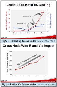
Technology scaling has made positive impacts on device performance, while creating challenges on the interconnects and the fidelity of its manufactured shapes. The process dimension scaling has significantly increased metal and via resistance for advanced nodes 7nm and onward, as shown in figures 1a,1b. Similar to a fancy smartphone without a good wireless carrier quality (4G/LTE or 5G), a higher performance device is deemed an unattractive option as it needs to be accompanied by optimal wirings in order to minimize net delay attributed latency. Hence, to accurately measure design targets, capturing interconnect contribution during IC design implementation is crucial.

Challenges to parasitic extraction
From a designer’s standpoint, a good parasitic extraction solution should address accuracy, performance, capacity and integration aspects.

Accurate modeling of wire capacitances in an advanced node process is a non-trivial task as it is a function of its shape, context, distance from the substrate and to surrounding wires. It eventually leads to solving the electrostatic field in a region involving multiple dielectrics. The more heterogeneous design trend employing innovative and complex packaging has also necessitated the augmentation of existing extraction techniques with 3D-IC modeling capability (see figure 1c).
As design size is growing, both the extraction file size and turn-around time increases –to reflect the jump in design net count, extracted RC networks size and its associated physical representation or layers handling. Capacity works both ways: the extraction tool of choice should be capable of absorbing a large design, do the extraction and produces an extraction file that is reasonably compact to be back-annotated in downstream timing analysis stage. All of these should be done fast, too.

Apart from managing route resources or interconnect (by means of pre-routes, layer assignments and route blockages), having an accurate and robust parasitic extraction technology is also essential in helping to pinpoint hot-spots due to ineffective utilization of wires or vias, and any potential signal integrity related issues. The extraction step should be interoperable with either the analysis or the optimization tools that will consume the parasitics data points.

Modeling, extraction accuracy and xACT
Both device and interconnect modelings hold critical role in providing accurate parasitic values. With device architecture transitioning to non-planar, multi-gate architecture such as FinFET and the upcoming the Gate All Around (GAA) structures, the current density and parasitic capacitance between the gate and source/drain terminals is expected to increase with further technology scaling.

During the micrometer process technology era, field-solver techniques for capacitance extraction was reserved for correlation purposes as it provided good results accuracy but was computationally expensive. We were also accustomed to labeling 2D, 2.5D, or pseudo-3D modes to RC extraction. Recently, there are many field-solvers and its variations noted (from finite element to boundary element based and to the most recent floating random-walk method). While accuracy is traditionally achieved through discretization of the parasitic equation by means of table lookup, such approach is inadequate with the increased layer and design complexity.

Calibre xACT™ is Mentor’s high-performance parasitic extraction solution. It combines fast, deterministic 3D field solver and accurate modeling of physical/electrical effects of complex structures/packaging used in advanced nodes –to deliver needed extraction accuracy, including rotationally invariant total and coupling capacitances.

In order to address RC extraction of heterogeneous design such as a 3D-IC with FOWLP (Fan-Out Wafer-Level Packaging), xACT applies a 3D-IC modeling by taking into account two interface layers between the neighboring dies as shown in figure 2. It captures their interaction and creating an ‘in-context extraction’ which offers highly accurate and efficient extraction results –with 0.9% error and 0.8% for the total ground capacitance and total coupling capacitances, respectively.

xACT also handles new interconnect modeling requirements at all layers such as accounting potential shift in BEOL due to multi-patterning impact on coupling capacitance, MOL contact bias modeling, Line-End Modeling (LOM), etc.

Extraction size reduction techniques
SPEF/DSPF and log files are notoriously ranked top on IT’s disk-space screener list. These files though normally retained in a compressed format, are still huge and can strain not only disk space, but also downstream simulators’ capacity –so reducing the parasitic size while not losing the overall accuracy is key.

Unlike some parasitic extraction methods’ reliance on the use of threshold or tolerance value as basis for parasitic size reduction, xACT is resorting to a more efficient reduction mechanism known as TICER (TIme Constant Equilibration Reduction). Electrically-aware TICER produces a smaller RC network while controlling the error. This feature can be used across design flows (analog, full-custom and digital sign-off).

A trial on a 128K SRAM design shows 30% faster timing simulation a parasitic netlist with TICER reduction (figure 3) when compared to an unreduced netlist, while the simulation error was within 2% compared to the unreduced netlist (figure 4).

Multi-corner interconnect extraction is usually a requirement for cell characterization and design sign-off as they have to be performed across multiple process corners. The introduction of multi-patterning at advanced nodes adds even more corners. For example, due to multi-patterning at 7 nm, the original nine process corners gets expanded to more than a dozen, since each has one or more multi-patterning (MP) corners. Instead of running each process corner separately –which is costly, xACT performs simultaneous multi-corner extraction, in which all process, multi-patterning, and temperature corners are extracted in a single run. The user specifies the desired combination of corners to extract and netlist, which is done after a LVS run.

Speed, capacity and integration
Because designs are also growing in complexity at each successive node, a big challenge for parasitic extraction at 7nm is processing the design and the necessary corners without incurring additional cycle time during the signoff phase. xACT solution handles all of these complex modeling requirements and utilizes a net-based parallelism with multi-CPU processing to deliver fast and accurate RLC parasitic extraction netlists. It enables full-chip extraction of multi-million instance nanometer design with multi-threaded and distributed processing architecture.

Advanced technology scaling has also introduced increased geometrical variabilities induced by the uncertainties in the manufacturing processes. Such variations of the manufactured devices and interconnect structures may cause significant shift from their design intent –the electrical impact of such variability on both the adjoining devices and interconnects should be assessed and accounted for during signoff.

Performance is multidimensional. From implementation perspective, design performance is not a function of the characterized library and wire choices only, but might be influenced by signal integrity induced delay. On the other hand, reliability analysis such as EM and self-heating are becoming more common and augmented as part of sign-off, xACT provides device location information to these tools to ensure current density violations can be accurately identified and resolved. Subsequent corrective actions such as via doubling and wire spreading can be taken to reduce current density occurrence.

The Calibre xACT platform also uses foundry-qualified rule decks in the Calibre SVRF language, and is interoperable with the Calibre nmLVS™ tool and with industry-leading design implementation platforms.

For more details on Mentor’s Calibre xACT, please check HERE.


Solving and Simulating in the New Virtuoso RF Solution

Solving and Simulating in the New Virtuoso RF Solution
by Tom Simon on 10-30-2018 at 12:00 pm

Cadence has done a good job of keeping up with the needs of analog RF designs. Of course, the term RF used to be reserved for a thin slice of designs that were used specifically in RF applications. Now, it covers things like SerDes for networking chips that have to operate in the gigahertz range. Add that to the trend of combining RF and digital blocks onto one die or into the same package and the scope of analog RF designs expands pretty rapidly.

Nevertheless, there were a few noticeable holes in the Cadence solution when it came to addressing RF designs. In the case of simulation, different parts of the design often resided in Allegro SiP or Virtuoso, so integrating and managing pre and post layout simulation was problematic. The other hole for RF users were the options available for EM solver based model generation and simulation. However, Cadence has expended a lot of effort to resolve these issues in their new Virtuoso RF Solution, and the results look pretty promising.

I had a conversation with Michael Thompson, RF Solutions Architect at Cadence, about the work they have recently done to improve the entire solution. His first point was that it used to be OK to do design separately, but changes in IC and package design mean that many more things are being combined and need to be looked at in a unified way. Thus, Virtuoso and Allegro SiP should to work together for RF designs. This created a requirement for lowering the barriers to exchanging design data between the systems, creating free bidirectional data exchange. They added the ability to concurrently use multiple technologies for simulation and layout. The key is to have one golden schematic for the entire design, including the package and multiple die, inside of Virtuoso.

The other hole they needed to plug was integration with EM solvers to make the flow seamless. Previously Cadence relied on a patchwork of external solvers integrated with SKILL code through the Connections Program. Of course, Cadence had their FEM solver that came in through the Sigrity acquisition. However, it was really targeted at board and package level problems as evidenced by its SiP integration. The majority of IC solvers are Method of Moments. Cadence struck a partnership with National Instruments to integrate their AWR Axiem tightly into Virtuoso. At the same time, they also created a path for Sigrity in the IC flow.

With seamless integration for extraction and simulation set-up, the ease of adding RF models for critical structures has improved dramatically. The models are S-parameter, but Spectre-RF has also improved its S-parameter handling. As a circuit’s design progresses, designers can move from QRC, to FEM and MoM, while keeping each of these as separate extracted views. The Hierarchy Editor allows swapping models for the simulation runs.

For the Virtuoso RF solution, Cadence has also been working on new device models. One example that Michael brought up was GaAs models.

Their solution brings together package and IC design into one environment where difficult RF design problems can be solved more easily. This new solution was shown for the first time at IMS. Ensuring that teams working on the package and on the IC can share data and analysis results makes sense with the growing complexity of RF designs. For more information on the new Cadence Virtuoso RF Solution, I suggest looking at the solution page on their website.


A Smart Way for Chips to Deal with PVT Issues

A Smart Way for Chips to Deal with PVT Issues
by Tom Simon on 10-30-2018 at 7:00 am

We have all become so used to ‘smart’ things that perhaps in a way we have forgotten what it was like before many of the things we use day to day had sensors and microprocessors to help them respond to their environment. Cars are an excellent example. It used to be commonplace to run down your battery by leaving your lights on. Now cars are smart enough to turn them off if left on too long. Even better illustrations are how cars adapt to driving at elevation or warm up smoothly when cold. There were simple mechanical gizmos that tried to compensate for operating conditions, but they were prone to malfunction or operating poorly. The use of monitoring has completely changed how reliable things are and how well they can adapt to changing conditions.

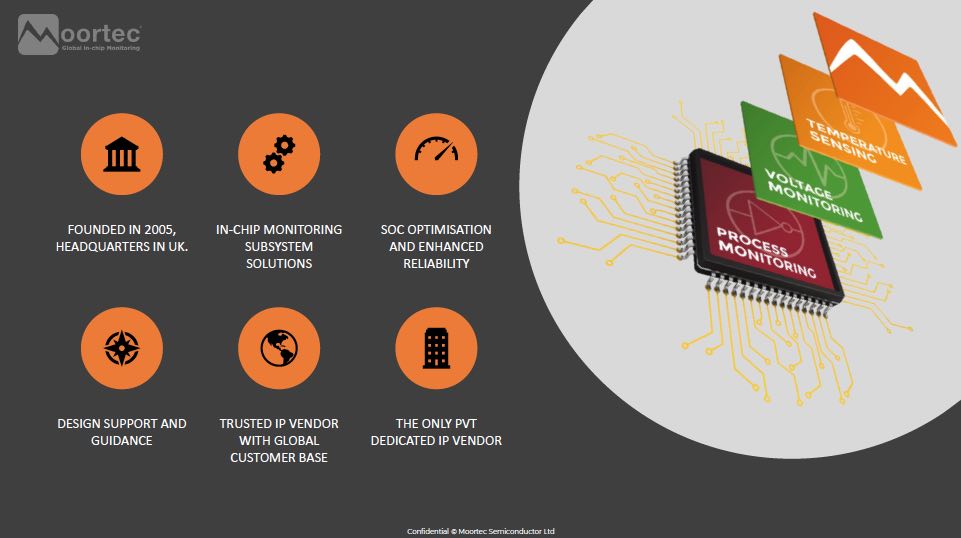
What we sometime fail to appreciate is that SOCs need to be smart in the same way. If my car can adjust the fuel mixture to compensate for temperature or oxygen levels, then why shouldn’t ICs adjust automatically for things like metal variation, operating voltage or even local temperature levels? If ICs can be made smart then performance, reliability and even yield will improve. Moortec is an IP provider that has been focusing on in-chip monitoring for almost a decade. They have sensors and controllers that can be embedded in SOCs during design that can help measure, adjust and compensate for a large variety of issues that occur in ICs during operation and over time as they age.

The most basic use of PVT sensors is to expedite and facilitate testing. Chips can be rapidly binned and proper operation can be verified by checking internal performance characteristics. However, there is a lot to gain by moving beyond using in-chip sensors for test and using them to dynamically manage chip operation.

Chips endue stress from higher self-heating with newer process nodes and the higher densities that they bring. Electrical overstress, electro migration, hot carrier aging, and increased negative bias temperature instability all threaten IC operation. Likewise, IR drops caused by increased gate capacitance, more resistive metal, and even supply issues can cause performance degradation or even failure. Additionally, process variation is harder to control because of new variation sources, multiple thresholds and the effects of ageing.

Moortec has been working on this problem since 2010, with their focus on in-chip monitoring systems. They have put together a system that uses several different sensor IP blocks that can be placed one or more times on the die. They tie these sensors together with a PVT controller which can be used to support DVFS/AVS, clock speed optimization, silicon characterization, and increased reliability and device lifetime.


Their process monitoring IP block uses multiple ring oscillators to assess device and interconnect properties. With the results of this sensor it is possible to perform speed binning, age monitoring and report timing analysis.

The voltage monitoring IP block is extremely versatile. It can monitor IR drop, core and IO voltage domains, and facilitates AVS. At the same time, it also helps monitor the quality of the supplies. It is useful in detecting supply events, perturbations, and supply spikes. An interesting feature is the ability to use one instance to monitor multiple supply domain channels in FinFET nodes.

The last leg of the triad is their temperature sensor. It has high accuracy and resolution and offers a number of testability features together with variable sampling modes to allow higher sampling rates if needed for performance.

High reliability and performance both require in-chip monitoring. In each of the critical markets for semiconductors today, it is necessary to squeeze out every ounce of performance while ensuring reliable operation. In safety critical systems such as ADAS, monitoring proper functioning and detecting age related failures is mandatory. Mobile devices need to operate at the lowest power possible, so DVFS is almost always used. In servers, high operating speed generate significant heating which even when minimized can still affect chip operation.

Moortec’s solution looks like it offers IP that is easily deployable to make chips smarter. I just wish that my parents’ carbureted Pontiac I drove in high school had the smart features that today’s technology provides. However, talking about that is a little bit like complaining about what a hassle dial phones were back in the day. That said, it seems inevitable that all chips will be smart soon enough. More information about
Moortec’s in-chip monitoring IP is available on their website.