By now it is pretty clear that everywhere outside of China and South Korea human beings are doing a lousy job of “social distancing,” locking down, and sheltering in place. This is unfortunate because experts agree that only a complete lockdown will stop COVID-19 from infecting millions, continuing to kill thousands, overwhelming healthcare systems, and devastating the global economy.
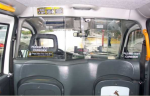
Nowhere is this failure to shut down more apparent than in our willingness to allow taxis and ride hailing operators to continue to operate without safety partitions. This lax approach to COVID-19 policy must end.
The onset of COVID-19 has exposed an essential weakness of the transportation gig economy – the lack of safety partititions in ride hailing vehicles. In fact, the pervasive competitive influence of ride hailing operators such as Uber and Lyft in the U.S., led, in 2016, to the New York City Taxi and Limousine Commission dropping the requirement for a safety shield in yellow taxis.
The NYTLC predicated its decision on the need for taxis to be able to be more personal in order to more effectively compete with Uber and Lyft. What the agency seemed to have forgotten at the time, five years ago, is that prior to the institution of the safety shields more than 40 taxi drivers were being murdered every year. The installation of safety shields nearly completely eliminated these fatal encounters.
We now have potentially fatal encounters of an entirely different kind – drivers, who may be infected with the coronavirus, driving passengers who may be infected with the coronavirus, creating a powerful vector for spreading the disease across the landscape. While taxi and ride hailing business is down 60%-70% – drivers can still handle 10-20 fares a day any one of which or all of which may be or become “spreaders” of the disease.
What is the response from Uber and Lyft? Encourage drivers and passengers to wash their hands, wear masks, don’t touch your face, and, my favorite: ROLL THE WINDOWS DOWN! Seriously? Roll the windows down as an anti-COVID-19 measure?
Serious social distancing or lockdown policy must forbid the use of taxi or ride hailing service providers unless the individual operators have a certified safety shield permanently installed in their vehicles. There is a reason we have regulatory agencies overseeing the taxi industries. The lives of passengers and drivers are at stake. There are well understood safety measures in place that were created decades ago when drivers were being routinely assaulted and, in some cases, killed by anonymous passengers.
Airlines have been shut down. People are too close for safety on planes and planes should not be transporting potentially infected passengers anywhere – domestically or internationally – with the exception of exceptional circumstances.
Public transportation networks have been shutdown or are offering reduced service. Like planes, passengers are in too close proximity on trains and buses and there are too many touchable surfaces to guarantee safety.
Taxis and ride hailing operators MUST shut down, unless their vehicles are equipped with certified safety shields. There is no excuse. Allowing these operators to continue to function as if it is business as usual is criminal.
It is not unlike retail clerks. We are beginning to hear stories of retail clerks at pharmacies and grocery stores testing positive and, in at least one case in Italy, dying. Supermarket chains in the U.S. are in the process of erecting Plexigas shields at their cash registers to protect their clerks. Like post-911 airport security – these Plexigas shields are likely to become a permanent fixture at your local grocery store.
Partitions actually serve many functions as evidenced by the Rolls Royce Phantom Partition Wall which includes an intercom and a pass-through for notes (but big enough for a weapon). Notes Project Manager Doug Claus: “The Phantom is the vehicle of choice for ‘social distancing’ in the ultimate luxury sector.”
Claus says the electrochromatic screen on the Phantom Partition Wall changes from transparent to opaque at the touch of a button. There is an integrated intercom system which mutes the front compartment audio system as the owner’s call is patched through immediately, but requires the owner to accept a call from the front compartment, so as not to be unduly interrupted.
The partitions implemented by taxis and ride hailing operators may not rise to the level of luxury and performance of the Phantom Partition Wall, but the masses requiring transportation beyond the luxury sector are entitled to the same level of safety and security. Uber, Lyft, Gett, Grab, Via, Yandex, DiDi and the rest of the ride hailing operators – and yellow and black and green and blue taxis – must have partitions to operate safely in the time of COVID-19. To proceed otherwise is to court disaster in the name of business as usual.
For further insight into mobility strategies, regulations, decision making, please register for and join a Strategy Analytics Webinar, for this Thursday, March 26th:
Swiss MaaS: The Evolution of Mobility in Switzerland, Europe and the World