
It is pretty common for physical layout to work from a flattened hierarchy for blocks or even full chips, even though the front-end design starts with a hierarchical representation. This was not always the case. Way back when, the physical layout matched the logical hierarchy during the design process. Of course, this led to all kinds of problems with placement and routing congestion. When the split was made to break hierarchical consistency from the front end to the back end it caused endless headaches. Even today, with most flows ironed out pretty well, there are still pain points in using a flat physical representation. Nevertheless, the advantages outweigh the drawbacks.
At the same time, some operations that were traditionally performed on flat designs have matured and can be done hierarchically for improved efficiency. A good example of this is DFT, where Mentor has introduced its Tessent Hierarchical DFT and Memory BIST solutions. The obvious advantage is that DFT and memory BIST can be inserted at the block level, and then driven in the finished design through hierarchical connections to each subunit. When changes are needed, only the affected blocks require modification.
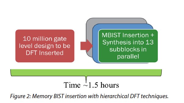
So, what happens when the physical design is flat, but the design is so large that performing DFT and inserting memory BIST takes too long? This is the issue that a recent Mentor case study examines in the flow used for an ON Semiconductor design with ~10 million gates and 300 memory instances. Using a flat DFT and memory BIST methodology took 9 hours, which meant that a design iteration could cost an entire day. ON Semiconductor worked with Mentor to devise a hybrid flow that let them keep their flat physical design and take advantage of the hierarchical efficiencies of Tessent Memory BIST.
The challenge was to take advantage of the efficiency of hierarchical memory BIST on a flat design. Overlaid on this were the usual considerations for designing and grouping memory BIST controllers. Physical proximity plays a big role in deciding which memories can share controllers. Because it is better to test memories at their native speeds, grouped memories should be in the same clock domain. Running all memory test concurrently might exceed the available power dissipation capabilities, so decisions are necessary about which tests can be run in parallel. There are also algorithm and repair issues to sort out.

The solution that Mentor and ON Semiconductor arrived at was to partition the final flat physical design into 13 submodules and adding memory BIST to them using Tessent’s hierarchical flow. The test insertion time for each submodule is about 1.5 hours. Because they can be run in parallel, the overall runtime for the full chip went from 9 hours to 1.5 hours. Scan chain insertion was still done at the top level, however, DRC verification can be done at the submodule level, saving even more time – ~25%. IJTAG (IEEE 1687) was used at the chip level and Tessent MBIST was used to generate memory BIST patterns.
ON Semiconductor was pleased with this approach because they gained many of the advantages of a hierarchical test flow but did not have to go back and redesign the physical implementation. As I have said before, I like real world examples of how specific tools are beneficial. In this case the participation of ON Semiconductor shows the practical real-world value of the Tessent hierarchical flow in an interesting hybrid application. More details of the methodology are available in the case study which can be downloaded from the Mentor website.
Share this post via:


Comments
There are no comments yet.
You must register or log in to view/post comments.