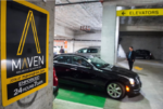
webinar banner2025 (1)

Crashing the Mars Rovers!!! Actel and Aerospace Corp

Crashing the Mars Rovers!!! Actel and Aerospace Corp
by John East on 09-30-2019 at 6:00 am

In early 2003 Actel announced a new product family:  RTSX-A.  It was a family of antifuse FPGAs aimed at the satellite market.  Customers had known for a long time that it was coming and there had been prototypes available for many months.  Our space customers loved the product.  This was going to be a big win for us!  One of the first programs to use the product was the Mars Rover program. There were four Mars Rovers made:  two went to Mars and two lived in a huge sandbox in Pasadena which allowed scientists to emulate conditions on Mars.  The two that went to Mars were named the Spirit and the Opportunity.  NASA’s plans were that the Rovers would live for three months before succumbing to the treacherous Mars environment. The Spirit launch was on June 10,  2003.  It would take the Spirit about eight months to make the trip to Mars.  The Opportunity was launched a month later.

Shortly after the launch we got reports from potential customers of a few RTSX-A burn-in failures in their labs. What’s burn-in?  It’s a test that assures the user that a part that starts out good will stay that way after being in actual use for some time.  Testing parts for one week at extremely high temperatures is the normal way to assure that they’ll last a long time at normal temperatures. We hadn’t seen failures with our first tests, but when we got those reports from our customers, we looked harder.  When we looked harder, we saw some failures on occasion.  We would burn-in around 100 units at a time.  Sometimes we would get 1 or 2 failures.  Sometimes none.

A small number of failures is worse than it sounds! A typical satellite would cost in the neighborhood of 100 million dollars in those days.  The Mars Rover project cost much, much more than that. The Mars Rover project used the RTSX-A.  Uh oh!!

Satellites can’t be repaired. If one IC fails, the cost of the entire project may well be flushed down the toilet.  Worse, there wasn’t just one RTSX-A part in each Rover.  There were, as I recall, 38.  That meant if there was a 1% chance that one particular Actel part would fail, there was a 38% chance that one of our parts somewhere in the Rover would fail.  (My math isn’t quite correct here, but you get the point) It was clear something wasn’t quite right, but we couldn’t figure out what.

The Mars Rover program was by no means the only program planning to use our parts.  There were many others! Word got around the space community. Many customers weren’t sure if they dared to launch their satellites. They looked to us to tell them it was OK.  We couldn’t. We just didn’t know. We couldn’t figure it out. A few skeptics thought we were covering something up. We weren’t. It was a very tricky problem. We were working hard on it, but we just didn’t understand what was going on.

Then, I got a call from Bill Ballhaus, the CEO of Aerospace Corporation. Aerospace Corporation operates a federally funded research and development center. They provide technical guidance and advice on all aspects of space missions to military, civil, and commercial customers.  Dr Ballhaus asked me to come to the Aerospace headquarters in El Segundo to discuss “the reliability problem with Actel FPGAs”

I, of course, accepted the invitation, but if you had offered me a choice of going to this meeting or getting a root canal on every tooth, my oral surgeon would be a richer man today.  The invitation appeared to be for a one-on-one meeting between me and Dr Ballhaus.  I planned on going by myself, but our VP of Technology,  Esmat Hamdy, saw it differently.  He didn’t quite trust my technical savvy.  He thought that, if the meeting turned out to have a lot of technical content, I might not be able to answer all the questions well.  So —  Esmat insisted on coming with me. Bless his heart!

We flew to LAX and then took a quick cab ride to Aerospace.  It’s about a mile from the airport. A secretary led us to a conference room  — except it was more like a sports arena.  There was a long rectangular table that probably sat 15-20 people.  Then there was an aisle circling those seats.  But on the other side of the aisle, there was an elevated set of chairs circling the table below.   There were maybe another 20-25 chairs in that set.  In total I would guess 30 or 40 chairs.    All but four were full.  Not full of just anybody   —  but full of PhDs.  Full of experts in any aspect of integrated circuits that you could think of.  Full of technical wizards who all had at least double my IQ. One of the empty chairs was for Dr Ballhaus.  One for Esmat.  One for me.  We took our chairs and were ready to start the meeting but Dr Ballhaus said that we’d have to wait.  The last chair was for a high ranking Air Force general who had invited himself to the meeting.   The general was running late.  When he got there, there was plenty of bowing and scraping done.  He was the head honcho!!

They hammered into me just how important this was.  The Rover program cost about one billion dollars.  The Rovers had been launched. There would be no calling them back.  No fixing them. If they went bad, that would be a billion dollars flushed.  And worse, the Mars Rover project was by no means the only satellite project with plans to use Actel.  There were several military satellite programs related to our national defense as well.  Those folks were even more worried than the Mars Rover people.  They were not happy campers!!!  As you would expect — the general had zero interest in putting up military satellites critical to the nation’s defense that were likely to fail!!!!!  (That unhappiness earned me an invitation to meet later with Peter Teets,  the Undersecretary of the Airforce, in the most secure area of the Pentagon.  Mr Teets wasn’t a happy camper either, but that’s another story.)

Back in Mountain View, we were breaking our picks.  We didn’t always see failures. When we saw them, there weren’t many.  That makes the problem harder to solve.  We suspected what we called the programming algorithm. The oversimplified explanation of programming an antifuse is this —  put a high voltage across it,  the dielectric will rupture and the antifuse will be a conductor for the rest of time. — In fact, it’s much trickier than that.  There are a lot of knobs to turn.  How high should the voltage be?  How much current should flow through the fuse?  How many times should you repeat what you’ve done?  How long should you apply the voltage?  How much should you “soak” the fuse? We would twist some of these knobs, come up with a new algorithm, and voila.  No failures!!!   Problem solved,  right?  Wrong!!!  The next time we’d run exactly the same test, there would be one or two failures.  We were completely perplexed!

The first Rover (the Spirit) was launched prior to suspicions that we might have a reliability problem. Then came the reliability worries. And then, around New Years when the reliability concerns had become rampant, the Spirit reached Mars. It was a big deal in the press.

The Spirit Lands on Mars!

It’s working fine!!

It was on the front page of every newspaper. Boy.  Did we ever feel good.  The Spirit was working perfectly!!!   …..……   But then  —  one week later —-

The Spirit Fails!!

The Spirit went bad.  That was on every front page too, but in bigger letters.  Was it the Actel parts? We didn’t know, but in my judgement … it could well have been. I was terrified!  I could picture the headlines when it was determined that Spirit failed because of an Actel part.  I could picture the lawyers lining up to file lawsuits against us.  I could picture the process servers skulking in the bushes waiting to spring out and serve me with subpoenas.  It wasn’t pretty!!  In fact, it was really, really ugly!! When I went home after work that night, I opened a bottle of wine and drank the whole thing by myself.  I like wine ……  but not a whole bottle.  My advice?   —  Don’t do that!!!  It didn’t work out well!!

Luckily, I was wrong. The Actel parts were not at fault.  After a week or so, NASA figured it out.  It was a software problem that was fixable by uploading new software.  They fixed the Rover, and independently we tracked down our problem and fixed it. To my knowledge Actel (Now part of Microchip) has never experienced a failure in space.

Scientists had planned for the Rovers to live for three months.  When did they actually die?  The Spirit lived for 6 years.  The Opportunity 14.

Epilogue

Somewhere around the year 2000 our board of directors asked the question, “John, how long do you plan to stay on as CEO?”.  My answer:  “I’ll retire no sooner than my 65th birthday and no later than my 66th”.  When you’re 55,  65 seems really old, doesn’t it?  Well, ten years later along came my 65th birthday.  January 20, 2010.  Funny thing.  By then 65 didn’t seem so old.  Still – all in all it was the right thing to do. We released an 8K (that’s the document that public companies use to disclose relevant information.) saying that we were beginning a search for a new CEO immediately and that we planned to complete the search and appoint a new CEO within a year.

We spent several months on the search.  There were some ups and downs – but bottom line, we made zero progress.  We were back to square one.  Then came a surprise. We received an unsolicited and unexpected offer to buy us out from Microsemi  — an Orange County based semiconductor company that I was barely aware of.  We discussed it at length!

Why would we be interested in selling?  We were in the middle of trying to transform ourselves from an antifuse company to a flash company.  I firmly believed that it could be done (In fact,  it was done!!!  See my week # 16, “From AMD to Actel”),  but it was obvious that it was going to take a long time before we finally started to see the results on our bottom line.  The bottom line matters!!  Shareholders want high stock prices!! And — for a company our age, the stock price is determined by the bottom line.

Dan McCranie (Who we had recently appointed chairman of the board) went to Orange County and met with the Microsemi CEO, James Peterson.  After some negotiations, Peterson offered a price that was higher than we believed we would be able to command consistently in the foreseeable future.  After a few vigorous board discussions,  we decided that we owed it to our shareholders to accept the offer.  We did. On November 3, 2010 Actel became part of Microsemi Corporation and I rode off into the high tech sunset  –  unemployed for the first time in 45 years.

This is the last episode in the series.  I hope you’ve enjoyed reading them as much as I’ve enjoyed writing them.

See the entire John East series HERE.

# Mars Rovers, Spirit,  Opportunity, Actel, Microchip, Aerospace Corporation,  Bill Ballhaus, Esmat Hamdy  Microsemi, Dan McCranie


Fossil Fuels in the Crosshairs

Fossil Fuels in the Crosshairs
by Roger C. Lanctot on 09-29-2019 at 11:00 am

In the heat of a presidential campaign, especially one with 19 competing candidates, the contenders may get carried away in the interest of getting attention and, presumably, attracting supporters. Beto O’Rourke might be accused of such rhetorical excess for his call, in the third Democratic Party debate, for a mandatory Federal assault rifle buyback.

But fellow Democrat Senator Bernie Sanders may have beat Beto with his plan to pursue criminal charges against fossil fuel executives for, in the words of truthdig.com, “knowingly accelerating the ecological crisis while sowing doubt about the science to the American public.”

Sanders’ comments came during an MSNBC climate town hall hosted by news anchor Chris Hayes at Georgetown University last Thursday. Truthdig.com quotes Sanders:  “Duh, of course I would. They knew that it was real. Their own scientists told them that it was real. What do you do to people who lied in a very bold-faced way, lied to the American people, lied to the media? How do you hold them accountable?”

Over the subsequent din of shredding machines going into overdrive at the offices of the major oil companies could be heard the clacking of worry beads at the headquarters of the major car companies. Knowledge of climate change is one thing. Building a product collectively responsible for 1.2M highway fatalities globally and hundreds of thousands of premature deaths from emissions every year – with an aggregate estimated negative societal impact of more than $1T – is enough to give even Senator Sanders and former Congressman O’Rourke pause to consider their options.

President Donald Trump’s efforts to roll back emissions standards and fuel efficiency requirements are pulling back the curtain on some very unpleasant issues the automotive industry would rather not highlight. While the industry is wrestling with the challenges of connecting cars and the onset of autonomous driving and electrification, the specter of premature death and injury caused by motor vehicles with internal combustion engines is an ugly open secret the industry would prefer remain out of the spotlight.

President Trump has dragged the issue to the center of the stage in the interest, so he says, of helping to jumpstart automobile production. The subtleties of managing emissions and fuel efficiency while enhancing vehicle safety – a high wire act which the automotive industry has ably executed thus far – has clearly eluded the commander in chief.

Young people and old around the world have made their concerns known regarding climate change. Their ire is mainly focused, today, on legislators and politicians. It won’t be long before they turn on the fossil fuel producers. Car makers could well be next – as was clear from the presence of protesters demonstrating once again outside the 2019 Frankfurt Auto Show. The President isn’t helping.


Micron Mired in Murky Memory Market – Cutting Capex 30%- 2020 Challenging

Micron Mired in Murky Memory Market – Cutting Capex 30%- 2020 Challenging
by Daniel Nenni on 09-29-2019 at 10:00 am

  • Solid Quarter but soft Outlook
  • Recovery Slow- Future Cost Downs Harder
  • Demand slightly ahead of supply-Shelf Stuffed?
  • Bouncing along the Bottom of the Cycle

Results ahead of expectation but guide behind expectation
Quarterly results were slightly better than street expectations at $0.56 EPS and $4.87B in revenues however guidance is for $5B +-$200M in revenues and $0.46 +-$0.07 in EPS which is well below expectations. While there may be some normal “sandbagging” of forward looking guidance even with that assumption its an unimpressive guide.

Disappointment that we are not yet at low tide
Investors are clearly not happy that the guidance does not yet indicate a bottoming of business. The stock was priced to perfection and a quarter guide that suggested being past the bottom of the cycle was also baked in to the high valuation.

We have been saying for a long time that this will be a longer, slower, shallower recovery. Investor and analyst hopes had gotten way ahead of reality. The reality is that we still have excess supply and demand is lukewarm with a number of potential risks in the market that add to uncertainty.

Cutting Capex 30% in 2020, front end cuts are deeper than back end
The company said what we have heard before and have been talking about for a while now……Capital spending will be down by 30% in 2020 versus 2019. Worse yet, the spending will be more focused on back end , assembly and test as well as buildings and less on front end equipment.

If we had to guess we would bet that front end equipment purchases are down at least 40% maybe as much as 50% while back end may only be down 20% or less.

This is obviously very negative for Lam and Applied and to a lesser extent ASML and KLAC. This additional data point of front end being cut more than 30% is obviously incrementally a lot more negative than some analysts and investors had been hoping for.

Wafer starts still being cut, bit growth will come from technology advancement
Micron made it clear that they are still idling capacity and wafer starts continue to come down as machines come off line as plugs are pulled. They said that bit growth will come from density (technology) increases not wafer start increases and that technology increases are enough to keep up with the needed teenage demand.

This is something we have been repeating for a while now, that bit growth can be met with Moore’s Law. So we can read this as selected technology only purchases, focused on pushing Moore’s law forward.

Further cost reductions will be more difficult in 2020
The company was also very clear that the aggressive cost of manufacturing reductions seen in 2019 will not be repeated in 2020. It sounds as if we are past the “easy” technological advancements are are now into more difficult technology changes that will be slower, harder and more costly.

We would read this as the company telegraphing that gross margins will be harder to come by in 2020 as costs will not come down as quickly as pricing.

Is Channel Stuffing going on?…yes
We have been warning of potential channel stuffing going on as Chinese buyers may be stocking up on fears of being cut off or buyers who frequent Samsung may be concerned about Japan cutting them off from critical materials.

Micron said this was going on but could not quantify how much of demand was this “mirage demand” due to stocking up.

Continued progress on 1Z and 96/128 NAND
Micron has made excellent progress in moving the technology ball forward and executing on all these new fronts.

These many advancements are clearly why Micron has been able to keep costs coming down ahead of falling prices. In past cycles, price drops always got ahead of cost drops but Micron has done a better job in this down cycle.

This has kept the company in much better shape on a competitive basis than in previous down cycles. Micron is likely a lot more competitive with the industry leader , Samsung, and claims to be ahead in some aspects.

Huawei is still “No Way”
Huawei is still on the “verboten” list even though Micron has applied for permission. News coming out today makes it seem as if the odds of Huawei being taken off the entity list or waivers being granted seem very low.

We would assume little to no business from Huawei going forward. If somehow this changes we would consider it a lucky break.

Still in wait and hope mode…maybe less hopeful
Micron’s stock has been in “high hopes” mode as expectations for a recovery got well ahead of themselves along with the stock price. We will obviously see a return to the reality of a slow recovery out of a murky bottom with an ill defined turning point.

We could see the run up in overall semi stocks reverse a bit as the wind comes out.

The stocks
There will likely be a significant correction in Micron’s stock price which was well ahead of where it should have been.

If we are at a run rate of $2 per year in EPS and were closing in on a $50 stock price we are at a 25 multiple which is obviously hard to support even at bottom numbers. There is likely support at the $40 level but we would not be interested in buying unless and until we got back to a “3” handle.

Collateral Damage
We don’t expect any better report coming out of Samsung as they are in the very same memory market with similar dynamics plus the additional worry of the Japanese embargo and now what looks like yield issues on their 7NM logic side as well. Samsung obviously gets the same pricing as Micron and even though Samsungs costs are generally lower there is less of a differential in the current down cycle.

Applied and Lam could see a 40-50% cut in business from Micron in 2020, making an equipment recovery all that much harder. While ASML and KLAC are more associated with technology advances than capacity advances there will also see weakness though less as KLA has always been more foundry/logic driven.

It would not be unreasonable to expect a 10% haircut in Micron’s stock price from its recent peak and AMAT and LRCX perhaps a 3-4% cut.


GLOBALFOUNDRIES Ready for IPO in 2022?

GLOBALFOUNDRIES Ready for IPO in 2022?
by Daniel Nenni on 09-28-2019 at 6:00 am

Hard to believe but it’s the 10th anniversary of Globalfoundries. What a journey this has been. It truly has been an honor to work with GF over the years as they invested many billions of dollars in the fabless semiconductor ecosystem and added a colorful chapter in semiconductor history, absolutely.

We have written hundreds of articles about GF that have been viewed by more than one million people. GF also has a chapter in our first book “Fabless: The Transformation of the Semiconductor Industry” which, in the 2019 update, documents the appropriately named GF pivot of 2018.

GF CEO Dr. Thomas Caulfield keynoted this year’s “Future of Innovation” event. Today GF has more than 16,000 employees and $6B in revenue making them the second largest pure-play foundry and the largest “specialty foundry”.

Tom made some interesting points in his opening:

  • World economy $85T
  • Electronics Industry $2T
  • Semiconductor Industry $475B
  • Semiconductor Foundry $63B

It really is interesting to know that five semiconductor foundries support the majority of an $85T world economy. Seriously, take away semiconductors and what do we have besides fire and the wheel?

It is also interesting to know that (according to LinkedIn) there are only 521,816 people worldwide who list themselves as “semiconductor related” professionals. So, congratulations to all of the hardworking semiconductor people like myself who made this miracle we call modern electronics possible.

Tom rightfully pointed out that 75% of the semiconductor devices shipping today are based on mature technologies (12nm and above) which is where the GF pivot has focused them. Tom also highlighted that the current GF output of 2.3M wafers ($6B in revenue) can be easily expanded to 3M wafers with an expected revenue of $8B. This is not a giant leap, in fact, I think that revenues will be even higher based on the platform strategy that was outlined in the presentation.

Please note that the equation in the figure above is a product (x) versus a sum (+) meaning that if any one of the variables is 0 the result is zero. This plays directly to the fabless systems companies which is the richest customer segment for the foundries.

Tom mentioned 15 different platforms utilizing 14 application features and 1,000s of silicon proven IP which will result in thousands of specialized application solutions. Again, the target here is electronics systems companies that are making their own chips.

The most interesting news out of the conference however was that GF is planning a public offering in 2022.  I’m a big fan of disruptive moves and while the GF pivot of 2018 was not what I would call disruptive, this IPO certainly will be.

A technology company IPO is definitely a rite of passage into corporate adulthood as it comes with a healthy level of transparency. Given the open media (fake news) we have today it is far too easy to become delusional from PR gone wild. Wall Street however is less easily fooled if you are playing by their rules, absolutely.

The big swing here is the legal action GLOBALFOUNDRIES filed against TSMC and some of their top customers. If the Wall Street bankers can make a silk purse out of this sow’s ear some serious IPO money will exchange hands and Abu Dhabi can finally put this one in the win column.

The semiconductor industry is full of incredibly smart people and it is an honor to work amongst them. One thing I can tell you is that the moves GF has made since Tom took the helm have been rock solid so I would not bet against him, not today.


Chapter Twelve – The Future

Chapter Twelve – The Future
by Wally Rhines on 09-27-2019 at 6:00 am

Content of this book has focused upon predictability of trends in the semiconductor industry based upon past trends, experience and ratios.  What about newly emerging applications of semiconductors?  After all, the entire history of the semiconductor industry is driven by emergence of new applications.

Artificial Intelligence
One of the most exciting new applications affecting semiconductor technology is the broad adoption of AI related analytics. AI is not a new technology.  Figure 1 is the cover of High Technology magazine in July 1986.  I am the person on the left and George Heilmeier, former head of DARPA, is the one on the right.  We tried hard in the 1980s but the infrastructure had not developed to a level where AI would provide profitable opportunities.

Figure 1. Artificial Intelligence technology heavyweights of the 1980s

What’s different today? In the 1980s, we lacked the computing power to handle big data.   We didn’t have very much big data to analyze partly because there was no internet of things. More sophisticated algorithms were needed.  Most of all, there were no obvious near term ways to make money using AI.

Today we have overcome all these limitations.  AI and machine learning have taken on a life of their own.  They have become limited, however, by the processing power available.  Traditional von Neuman general purpose computing architectures are inadequate to handle the complex AI algorithms. The result: a new generation of computer architectures is evolving.

Figure 2 shows the trend in venture capital funded fabless semiconductor companies in recent years. In 2018, a new record of $3.4 billion total investment was set, far above the previous record of $2.5 billion in the year 2000.

Figure 2.  Venture capital funded fabless semiconductor startups

Venture capitalists have been focused on social media and software companies over the last twenty years.  Where is all this new money going?  The answer can be seen in Figure 3. AI and machine learning have dominated the fabless semiconductor industry investment by venture capitalists since 2012 with $1.9 billion invested.

What kind of chips are being funded?  The largest share is in the area of pattern recognition.  Chinese investments in facial recognition chips developed at companies like Sensetime and Face++ constitute a very large share.  There are seventy-five other companies developing chips for pattern recognition that have been funded by venture capital.  These include companies focused on pattern recognition for audio, smell and other applications.

Figure 3.  Venture funded startups since 2012 by application. AI and machine learning constitute the majority of applications

Beyond pattern recognition, the largest share of new fabless semiconductor companies are being funded for data center analytics or edge computing.

Edge Computing
Intelligence historically flows downhill (Figure 4). In the 1960s, mainframe computers dominated our computing capacity.  Dumb terminals connected us to our mainframe computing power.  By the 1980s, minicomputers were well established as an intermediate computing layer between the user and the mainframe.  Twenty years later, the personal computer became the local computing resource.  In another twenty years, the current environment has evolved.  Large cloud-based server resources handle the heavy computing but in between us and the cloud is the fog made up of gateways that collect, aggregate and locally process data.  Beneath that layer are the edge nodes in the mist, collecting and pre-processing the data.  As time passes, the lower layers will inevitably gain more intelligence as semiconductor technology allows us to build more intelligence into the local nodes. Those nodes will become increasingly complex as they incorporate disparate technologies – analog, digital, RF, MEMs, etc.  (Figure 5).  This creates major design and verification challenges.  Most of EDA history is focused upon digital logic and memory.  Edge nodes may require mixed technologies.  Simulating digital logic connected to analog, RF and other technologies is not easy.  A whole new family of EDA tools is required.

Figure 4.  Intelligence flows downhill

5G Wireless Technology
In the next decade, wireless communication will move to the next generation of technology, 5G.  This transition is more significant than past generations.  It affects a wide variety of the infrastructure beyond consumer communications.  Significant impact will be felt in applications involving industrial control, non-real time automotive analytics, urban infrastructure and much more.

One of the great opportunities for the semiconductor industry is the increased number of base stations required to support the infrastructure of 5G and the larger number of antennas in a phone. The number of semiconductor components required will grow dramatically as the world builds a 5G infrastructure. Connectivity to the cloud makes a wide variety of capabilities possible, especially in the factories of the world.  Gateways, which already generate more than three percent of worldwide semiconductor revenue, will be needed.

This connected world will be dependent upon more semiconductors for communications and computing.  For many years the semiconductor industry measured its revenue from the computing and communications industries which were each about 35% of the total.  Now the two are indistinguishable.  Seventy percent of the revenue in the semiconductor industry comes from one or the other or a unique combination of both.

Figure 5.  Diverse technologies like digital, analog, RF and MEMs will be required as edge nodes become more intelligent

Automotive Applications
During the last ten years, sales of semiconductors for automotive applications has increased to about 12% of the total semiconductor market as the electronic content of vehicles increased.  Some traditional electronic functions like engine control will not be needed in electric vehicles but there will be new requirements as well as the continued growth of infotainment and automotive driver assistance (ADAS) that require electronic controls.

Figure 6.  As of June 2019, 463 companies have announced intent to introduce electric cars or light trucks.  211 companies have announced autonomous drive programs

The number of companies planning to build electric cars or light trucks has now grown to 463, more than half of which are based in China (Figure 6).  Two hundred eleven companies have announced autonomous driving programs.  This number of suppliers is not needed and many, or even most, will drop out as we move closer to production. Meanwhile, one would expect an incredible bubble in demand for automotive ICs followed by a rapid decline.

It’s likely that no more than a dozen companies will lead the way in supplying the complex image processing subsystems required for autonomous vehicles.  It’s difficult to predict which ones will succeed but likely that companies that have not been traditional automotive OEMs will make up most of the total.

Other Predictable Futures
Lots of other technologies offer promise for growth.  Quantum computing is interesting because it has some capabilities like encryption that are not solved easily through other means.  The time lag for technologies like this tend to be longer than the evolutionary ones but they will eventually emerge in some form.

The history of the semiconductor industry is driven by major new applications.  Waves of growth were initiated by defense electronics in the 1950s, mainframe computers in the 60s, minicomputers in the 70s, personal computers in the 80s, laptops in the 90s and wireless communications in the most recent two years. Each wave has been accompanied by the emergence of new semiconductor competitors followed by a shakeout that leaves one supplier dominant and shuffles the top ten ranking of companies by revenue (Figure 10 in Chapter 5).

At the same time, the semiconductor industry, like most industries, moves back and forth from standardized versus customized solutions.  This has been referred to as “Makimoto’s Wave” after Tsugio Makimoto, former CEO of Hitachi Semiconductor, who popularized the phenomenon.  As we move into the third decade of the twenty-first century, the semiconductor industry is moving into a customization wave.  Standard von Neuman computer architectures that operate on a string of standard instructions have dominated the computer and semiconductor industries.  Architectures like the Intel 808X and ARM RISC will continue.  Domain-specific architectures tailored for specific tasks like facial recognition are emerging. There will be dozens more as AI and machine learning usher in new opportunities.

What should we consider as the future possibilities for the semiconductor industry? As we showed in Chapter 4, the semiconductor industry is likely to grow through evolutionary means through about 2040 or when demands for lower power or higher performance usher in a new technology for information “switching”.  Carbon nanotubes, bio-switches, or many other possibilities could fill in the switching learning curve of Figure 5, Chapter 3.  Chances are that this “switch” will happen gradually as the need arises for a new application.  In addition, non-silicon materials like Gallium Nitride, Silicon Carbide and other materials will take on increasingly important roles driven by need for characteristics like larger band gaps, i.e. roles like power switching, microwave communications and existing ones like solid state lighting.

Just as steel is still a primary material for construction one hundred fifty years after the booming growth of the steel industry, semiconductors will be at the foundation of business and technology growth for a long time.  Those of us who participated in the last fifty years of exciting growth of semiconductors are still surprised when we see our “mature” industry generate another wave of growth to accompany an emerging application.  I’m confident that there will be many more to come.


AI Hardware Summit, Report #1: Doing More to Cost Less

AI Hardware Summit, Report #1: Doing More to Cost Less
by Randy Smith on 09-26-2019 at 10:00 am

I recently had the pleasure of attending the AI Hardware Summit at the Computer History Museum in Mountain View, CA. This two-day conference brought together many companies involved in building artificial intelligence solutions. Though the focus was on building the hardware for this area, there was naturally much discussion around software and applications as well. The first session I want to summarize was presented by Dr. Carlos Macián, Senior Director, AI Strategy and Products at eSilicon.

When I saw an eSilicon presentation on the agenda, naturally I assumed it would be about their recently announced neuASIC™ IP platform. If you don’t know about that yet, you may want to read about their AI IP platform first. Instead, we were treated to a much broader presentation on controlling the total cost of ownership (TCO) of an AI hardware solution. The presentation was quite insightful and showcased just how much depth and experience eSilicon has when it comes to building these types of ASIC products.

TCO is an important concept. When deciding how to address the challenges of building a hardware solution for a specific AI application, one needs to understand how each decision affects the total cost of the product. Some decisions carry more cost in area (die cost), yield (die cost), effort (person-hours), quality (sales, reputation, returns, etc.), power (packaging and other costs) and so many other factors. The list of traits and their associated costs is quite long. Given that most companies should have a grasp of the common TCO drivers, this presentation focused on the key items to consider for state-of-the-art AI products.

From the slide above, you can see that AI designs for data centers have some familiar drivers that are exacerbated by the need to move to massive parallelism – hyperscale. Hyperscale computing refers to the systems and architecture in distributed computing environments that must efficiently scale from a few servers to thousands of servers. Hyperscale computing is used in environments such as big data and cloud computing – today’s massive data centers.

Carlos clearly explained the biggest challenges to AI hyperscale implementation, along with the enabling technologies that have been rolled out at several companies now. Recent announcements, such as Intel’s announcement at HotChips of their Lakefield processor built using Foveros 3D technology, are a clear sign that these technologies are available now. The challenge is to find a partner who understands all of these enabling technologies, something that eSilicon has already demonstrated.

The presentation then went on to focus on an example of solving these AI design challenges by utilizing one of the enabling technologies – 3D memory overlays. The presentation demonstrated if you stack parts of the solution vertically (e.g., xRAM, SRAM+IO, and compute) on different die in the same package that there are huge efficiencies to be gained. One dramatic gain is yield. Manufacturing several smaller die that can be stacked increases yield dramatically. In the example shown at the event, yield improved from 15.7% to 68.6%. This yield improvement provides a tremendous decrease in the cost of production and therefore a dramatic improvement in the TCO.

Despite the difficulties some will encounter in getting these hyperscale AI designs to function at a reasonable cost, I think eSilicon has shown it has the expertise to get them across the finish line. They also disclosed that they are already working with suppliers on the next set of challenges as the degree of scaling increases – new die bonding technologies, vertical signal density, thermal density, combined yield, and many others. I will be anxious to hear more on these items when eSilicon is ready to discuss them.

eSilicon seems well prepared to deliver AI hardware designs. You can learn more about their NeuASIC AI capabilities here. You can learn more about their 2.5D/HBM2 packaging solutions here. As I have mentioned before, as an IP vendor, I referred my licensees to eSilicon before where their success lead to us getting our clients to volume quickly. That is why I recommend them highly.


Virtually Verifying SSD Controllers

Virtually Verifying SSD Controllers
by Bernard Murphy on 09-26-2019 at 5:00 am

Datacenter storage

Solid State Drives (SSDs) are rapidly gaining popularity for storage in many applications, in gigabytes of storage in lightweight laptops to tens to hundreds of terabyte drives in datacenters. SSDs are intrinsically faster, quieter and lower-power than their hard disk-drive (HDD) equivalents, with roughly similar lifetimes, though SDDs are (currently) more expensive. All appealing characteristics in a datacenter, perhaps in some suitable mix with cheaper HDDs. However there are other challenges with SDDs which make them in some ways more difficult to manage.

The memory cells inside an SSD wear out through repeated read/write/erase actions. Also writes to an SSD are at a page or block level (I’ll use block from here on for simplicity). You can’t just update one word; if you want to update a block already containing data you have to copy the block to SRAM, make the update, write the updated block to a new empty block and mark the original block for deletion. So far no problem, but those marked blocks have to be deleted so they can be recycled back into the system. That’s handled by garbage collection, which the controller will run in the background to avoid slowing down host reads and writes.

There’s an obvious challenge here when write-traffic becomes significant and scattered. Demand for new blocks to write can exceed the pace at which marked blocks are being deleted, in which case writing stalls waiting for garbage collection to catch up. And the supposed fantastic performance of the SSD takes a hit until the backlog is cleared. Which is not great for XaaS providers who want to claim reliably superior throughput.

In managing this problem, storage technologists have come up with a concept of predictable latency through which long tails in this distribution can be limited or even eliminated. Characterizing for this latency for a new controller design under a wide range of demands obviously requires running with a host model which will faithfully represent realistic datacenter traffic as a driver. Here Mentor have further extended their VirtuaLAB concept for Veloce emulation to provide an SSD reference lab, providing all the necessary virtualized operation components, allowing for a host OS such as Qemu, along with debug interfaces. The controller model runs on the Veloce emulator.

What I find particularly interesting about this is the natural fit of a virtualized version of the production storage interface working together with the emulator based DUT model. In the right contexts I’m a fan of ICE-based modeling, where you connect the emulator to real hardware to get all the real-life variability and odd behavior you will have to accommodate. But dealing with massively complex system loads by building large hardware test systems is impractical and inevitably very incomplete. Here virtualized modeling seems a better solution, given easier scalability to a wide range of applications. This is similar I think to the work VirtuaLAB interface Mentor have with Ixia/Keysight for network testing under a wide range of possible loads.

None of which means you’re going to get everything right pre-silicon in this kind of modeling. I’m not sure the old “first-silicon” goal applies any more in complex system devices. But you can shake out a lot of problems to ensure that validation with that first silicon build will be catching real-life corner-cases and not problems you should have caught in design.

You can read Mentor paper on this capability HERE.


High-Speed PHY IP for Hyperscale Data Centers

High-Speed PHY IP for Hyperscale Data Centers
by Tom Dillinger on 09-25-2019 at 10:00 am

A new designation has recently entered the vernacular of the computing industry – a hyperscale data center.  The adjective hyperscale implies the ability of a computing resource to scale corresponding to increased workload, to maintain an appropriate quality of service.

The traditional enterprise data center is often characterized as a back room warehouse of data processing and storage resources, with components of varying capacity and performance.  Customers commonly request resource allocations.  There is typically a long leadtime for hardware upgrades and resource growth.

Conversely, the hyperscale data center is by nature modularized and distributed.  The large cloud computing service providers are the models usually associated with hyperscale data centers, yet any IT operation with the following characteristics would apply:

  • modular facilities for power and cooling delivery

An analogy for the modularity of a hyperscale data center would be the construction of a housing development, where the overall facilities infrastructure is divided into phases, each consisting of individual building lots.

  • workload balancing

The footprint of the hyperscale data center assumes a typical thermal dissipation, to provide the facility cooling – planning for cooling to support maximal dissipation throughout the center would be cost-ineffective.  Balancing the utilization of resources involves thermal monitoring and support for workload relocation.

  • high availability

Hyperscale architectures include the capability to replicate/restart workloads across servers, in case of a failure.

The modularity in hyperscale data center architectures is associated with the ubiquitous server rack, as depicted in the figure below.

Figure 1.  Common server rack hardware configuration, illustrating optical module or Direct Attach Copper connectivity to the Top-of-Rack switch.  (Source:  Synopsys)

Top of Rack (ToR) is a common position for the network switch hardware.  The figure above also indicates the increasing network switch bandwidth required – e.g., 25.6 Tb/sec and 51.2 Tb/sec – and the network interface card technologies used in these rack configurations.

When describing the connection bandwidth, the key parameters are:

  • serial (SerDes) data rate and the number of SerDes lanes

The effective datarate is reduced (slightly) from the SerDes specification due to the additional bits added to the payload as part of the data encoding algorithm.

  • insertion loss and crosstalk loss of the connection medium, and the range of the connection

The key overall specification to achieve is the bit error rate (BER), which is determined by a number of factors – e.g., Tx equalization, Rx adaptation to optimize signal sampling time, and especially, the frequency-dependent insertion loss and crosstalk interference of the connection.

For these very high-speed data rates, individual specifications for these losses are often provided (the loss acceptance mask versus frequency), for different configurations – e.g., chip-to-chip (short reach); backplane with 2 connectors (~1m), and Direct Attach Copper cable (~3m).  Increasingly, above a 100 Gbps serial rate, copper cabling in the rack may be displaced by low-cost optics and/or a transition of the network switch to a middle-of-rack (“MoR”) position.

I had the opportunity to chat with Manmeet Walia, Senior Marketing Manager for High-Speed PHY Development at Synopsys, about the characteristics of the hyperscale data center, the increased data communications bandwidth, and the ramifications of these trends on hardware design.

“There are several key trends emerging.”, Manmeet indicated.  “For improved efficiency, Smart network interface cards (“SmartNIC”) are being offered, with additional capabilities for network packet processing to off-load the host.”  

“The intra-rack bandwidth requirements are increasing – 56G and 112G Ethernet are required.”, Manmeet said.   The figure below highlights how these IP are used in support of various aggregate Ethernet speeds, using multi-lane configurations.  The targets for bandwidth between data centers are also shown below.

Figure 2.  Evolution of Ethernet speeds, targets for DC-to-DC bandwidth.  (Source:  Synopsys)

“Switch designs are integrating electro-optical conversion and optical fiber connectivity for the Ethernet physical layer even in medium- and short-range configurations.  Inter-rack and data center-to-data center bandwidth must also increase to accommodate the network traffic.”

Manmeet provided the figure below to illustrate how electro-optical conversion is transitioning from a distinct network card module to an integral part of advanced packages, with optical fiber used locally.  (The electrical SerDes signal conditioning retiming functionality required at high data rates is thereby eliminated.)

Figure 3.  Electro-optical conversion transition from a module to an integrated function.  (Source:  Synopsys)

He continued, “The 56G and 112G Ethernet communications requires PAM-4 signaling – conventional NRZ signal transitions for these networking applications maxes out at 28G.”

Figure 4.  PAM-4 Signaling Eye Diagram and Test Challenges.   (Source:  Teledyne LeCroy)

Briefly, PAM-4 signaling implies there are 4 different possible voltage levels to be sensed at the center of the signal eye.  The PAM-4 signal sensing window is therefore 1/3rd of the NRZ (PAM-2) height.  The linearity of the 4 signal levels is a critical parameter.

As with an NRE serial signal, minimizing crosstalk noise is crucial, especially with the reduced voltage sense differences with PAM-4.

The time sampling in the center of the eye opening for the PAM-4 signal is more complex, as well.  The jitter at the edges of the eye is magnified in PAM-4, due to the varying transitions between individual levels in successive unit intervals.  Separate Tx and Rx clock sources are used for training and auto-negotiation, potentially on a per-lane basis.  Additionally, there is a common requirement to support varying speed settings, again potentially for each lane.

The IEEE 802.3cd working group is establishing 56G/112G Tx/Rx signal specifications and PAM-4 standards for various network topologies, from ultra-short to long-reach, and for shielded/balanced copper and optical fiber cables.

“What’s new in the Synopsys PHY group?”, I asked.

Manmeet replied, “At the TSMC Open Innovation Platform symposium, we are highlighting our N7 56G and 112G PHY IP.  We are also providing reference design evaluation hardware and software evaluation platforms for customers.”

Manmeet included the following roadmap for large network switch SoCs, integrating 256 lanes of the 56G and 112G PHY’s.

Figure 5.  Example configuration of high-speed PHY’s, for large network switch SoC designs.  (Source:  Synopsys)

“The 56G PHY IP is provided in an X4 lane increment.  The DesignWare Physical Coding Sublayer (PCS) enables the networking protocol to span a wide range of data rates.  The 112G PHY is offered in an X1 lane unit, with similar PCS flexibility.”

Figure 6.  Synopsys 56G and 112G Ethernet PHY implementation architecture.  (Source:  Synopsys)

Manmeet added, “Synopsys will be providing customers with additional design materials.  SoC physical layout PHY tiling and power delivery recommendations are included, based on the results of our package escape studies.  IBIS-AMI models are provided.  A software toolkit enables evaluation of Tx and Rx settings and signal eye characteristics.  A test chip evaluation card is also available.”


Figure 7.  Design kit materials for 56G and 112G IP evaluation:  IBIS-AMI model, software toolkit for lab evaluation, reference card.   (Source:  Synopsys)


Several trends are clear:

  • Computing models are rapidly adopting the characteristics of flexible “hyperscale” data centers.


  • The volume of network traffic demands an increase in bandwidth to 400G, enabled by the availability of 56G and 112G Ethernet PHY IP utilizing PAM-4 signaling, whether for short-reach or long-reach configurations, utilizing copper or optical cable physical layer interconnects. (For ultra-short reach interfaces, these Synopsys PHYs also include options to optimize power for low-loss channels.)


  • The complexities of integrating a large number of high-speed 56G/112G Ethernet PAM-4 SerDes lanes to optimize signal losses and crosstalk requires more than just “silicon-proven” test chips from the IP provider. A strong collaboration between customers and the IP provider is needed to adapt to the SoC metallization stack and to leverage the available software/hardware reference materials.


Here are links to additional information that may be of interest.

Synopsys 112G Ethernet PHY IP press release –  link.

Article:  “Shift from NRZ to PAM-4 Signaling for 400G Ethernet” – link.

Youtube video on 7nm 56G Ethernet PHY IP performance results – link.

Synopsys DesignWare 112G Ethernet PHY IP – link.


-chipguy


How Should I Cache Thee? Let Me Count the Ways

How Should I Cache Thee? Let Me Count the Ways
by Bernard Murphy on 09-25-2019 at 5:00 am

cache hierarchy

Caching intent largely hasn’t changed since we started using the concept – to reduce average latency in memory accesses and to reduce average power consumption in off-chip reads and writes. The architecture started out simple enough, a small memory close to a processor, holding most-recently accessed instructions and data at some level of granularity (e.g. a page). Caching is a statistical bet; typical locality of reference in the program and data will ensure that multiple reads and writes can be made very quickly to that nearby cache memory before a reference is made outside that range. When a reference is out-of-range, the cache must be updated by a slower access to off-chip main memory. On average a program runs faster because, on average, the locality of reference bet pays off.

For performance, that cache memory has to be close to the processor and therefore small; it can only hold a limited number of instruction or data words. As programs and data size get bigger, added levels of caching (still on-chip) became important. Each hold a larger amount of data at the price of progressively slower accesses, but still much faster than main memory access. These levels of cache were named, imaginatively, L1 (for level 1, closest to the processor), through L2, L3 and in some cases L4. Whichever of these is closest to the external memory interface is called the last-level cache.

Then we started to see multi-processor compute. Each processor wants its own cache for performance but they all need to work with the same main memory, introducing a potential coherence problem. If processor A and processor B read/write to the same memory address, you don’t want them getting out of sync because actually they’re each working with a local copy in their own caches.

To avoid chaos, all accesses still have to be synchronized with the central main memory address space. Delivering this assurance of coherence between caches depends on a lot of behind-the-scenes activity to snoop on locations written/read in each cache, triggering corrective action before a mismatch might occur.

For SoCs, Arm provides a cache-coherent communications solution between their processor IPs called the DynamIQ Shared Unit (DSU), solving the problem for fixed clusters of Arm CPUs. But for the rest of the SoC you need a different solution. Think of an AI accelerator for example, used to recognize objects in an image. Ultimately the image (or more likely stream of images) is going to come through the same memory path for processing by AI and non-AI functionality alike.

So AI accelerator accesses must be made coherent with the rest of the coherent subsystem. Arteris IP provides a solution for this through their Ncore cache coherent NoC interconnect which provide proxy caches to coherently connect non-coherent AI accelerators with the SoC coherent subsystem. You can do this with multiple accelerators, even multiple AI accelerators, a configuration which apparently is becoming popular in a number of devices.

Next consider that a number of these accelerators are becoming pretty elaborate and pretty big in their own right. Now the Ncore interconnect is not just a way to connect the accelerator to the SoC cache subsystem but a full coherent interconnect supporting multiple caches inside the accelerator.

This is needed because AI accelerators depend even more heavily on localized memory for throughput; a grid-based accelerator might have local cache associated with each processing element or group of processing elements. This coherent interconnect performs a similar function to the Arm coherent DSU but inside a non-Arm subsystem and using a NoC architecture which can more practically extend over long distances.

Then think further on those long distances and the fact that some of these accelerators are now reticle sized. Maintaining coherence directly over that scope would be near-impossible without significantly compromising the performance advantages of caching. What does any good engineer do at that point? They manage the problem hierarchically with multiple domains of local coherence connecting to higher-level coherent domains.

Finally and more back down to earth, what about the last-level cache, the one right before you have to give up and go out to main memory? Arteris IP provides the CodaCache solution here which can sit right by the memory controller. This is highly configurable for size, partitioning, associativity and even scratchpad memory to allow AI users to optimize tuning to the dataflow they expect to have with their AI app, perhaps to pre-fetch data they know they will need soon.

Caching has come a long way from those early applications. Arteris IP is working with customers in each of these areas. You can learn more about their Ncore cache coherent interconnect HERE and CodaCache HERE.


Semiconductors back to growth in 2020

Semiconductors back to growth in 2020
by Bill Jewell on 09-24-2019 at 11:30 am

Semiconductor market forecasts 2019 to 2021

The global semiconductor market is headed for the largest decline in 18 years. The market dropped 32% in 2001 when the Internet bubble burst. The 2019 decline should be around 15%, the third largest annual drop after 2001 and a 17% drop in 1985. The current weakness is largely due to excess memory capacity (DRAM and NAND flash) relative to demand. WSTS expects the memory market will decline 31% in 2019 while semiconductors excluding memory will decline only 4%. The market weakness is also due to an uncertain global economy and weakness in key demand drivers.

The second half of 2019 is showing signs of a turnaround. Below are the 2nd quarter 2019 revenues reported by major semiconductor companies and their guidance for 3rd quarter 2019. The non-memory companies showed revenue growth in 2Q 2019 versus 1Q 2019, ranging from 0.3% from Qualcomm to 16.2% from Nvidia. The memory companies (SK Hynix, Micron and Toshiba) experienced revenue declines, except for Samsung which grew 11.2%. A few companies expect healthy growth in 3Q 2019 revenues, ranging from 9.1% from Intel to 15.3% from STMicroelectronics. TI, Infineon and NXP project low single digit growth. Micron and Qualcomm expect revenue declines.

Recent semiconductor market forecasts call for 2019 to be decline about 13% to 15%. We at Semiconductor Intelligence are sticking with our June forecast of a 15% decrease. Forecasts for 2020 are in a relatively narrow range, from 4.8% by WSTS to 8% by Semiconductor Intelligence. For 2021, IHS Markit projects accelerating growth to 10% from 6% in 020. Our Semiconductor Intelligence forecast is for slightly slower growth in 2021 of 7% compared to 8% in 2020.

What are the drivers of the semiconductor forecast? One key is gross domestic product (GDP) which measures overall economic activity. The September forecast from Euromonitor shows a slowing of World GDP growth from 3.7% in 2018 to 3.1% in 2019. GDP growth picks up slightly to 3.3% in 2020 and 2021. The advanced economies (including the U.S., Euro area, UK, Canada and Japan) decelerate from 2.2% growth in 2018 to 1.7% in 2019 and 1.5% in 2020 and 2021. Two major factors behind the 2019 slowdown are the trade dispute between the U.S. and China and uncertainty over the UK’s exit from the European Union (Brexit). Growth is stronger in the emerging economies (including China, India, Russia, Southeast Asia and Latin America) at 4.3% in 2019, picking up to 4.6% in 2020 and 2021. Slowing growth in China is offset by accelerating growth in India, Southeast Asia and Latin America.

The two largest applications for semiconductors are smartphones and PCs/tablets. IDC projects smartphone units will decline 2.2% in 2019 after falling 3.4% in 2018. Growth should turn positive in 2020 and 2021 as 5G smartphones enter the market. Gartner expects the combination of PC and tablet units to decline 1.5% in 2019 after a 2.5% decline in 2018. The rate of decline will slow to 1.4% in 2020 and 0.6% in 2021.

Against this backdrop, the semiconductor market is unlikely to show strong growth in the next few years. Our Semiconductor Intelligence forecast of 8% semiconductor market growth in 2020 is largely due to a bounce back from the 15% decline in 2019. We expect growth to moderate to 7% in 2021 due to continued economic uncertainty and lackluster end equipment market growth.