RVN! 26 Banner revised (800 x 100 px) (600 x 100 px)

PCI Express in Depth – Data Link Layer

PCI Express in Depth – Data Link Layer
by Luigi Filho on 09-06-2020 at 6:00 am

PCI Express in Depth Data Link Layer

In the last article, i wrote about the physical layer, now let’s take a look in the next layer the data link layer.

The Data Link Layer serves as the “gatekeeper” for each individual link within a PCI Express system. It ensures that the data being sent back and forth across the link is correct and received in the same order it was sent out. The Data Link Layer makes sure that each packet makes it across the link, and makes it across intact.

The Data Link Layer adds a sequence number to the front of the packet and an LCRC error checker to the tail. Once the transmit side of the Data Link Layer has applied these to the TLP, the Data Link Layer forwards it on to the Physical Layer.

For incoming TLPs, the Data Link Layer accepts the packets from the Physical Layer and checks the sequence number and LCRC to make sure the packet is correct. If it is correct, the Data Link Layer removes the sequence number and LCRC, then passes the packet up to the receiver side of the Transaction Layer.

Now let’s talk about theses TLP’s.

The TLP stands for Transaction Layer Packet (TLP) and in the figure below is show a typical packet:

Now there is two main things we need to know:

  • Sequence Number – The Data Link Layer assigns a 12-bit sequence number to each TLP as it is passed from the transmit side of its Transaction Layer. The Data Link Layer applies the sequence number, along with a 4-bit reserved field to the front of the TLP.
  • LCRC – The Data Link Layer protects the contents of the TLP by using a 32-bit LCRC value. The Data Link Layer calculates the LCRC value based on the TLP received from the Transaction Layer and the sequence number it has just applied. On the receiver side, the first step that the Data Link Layer takes is to check the LCRC value. It does this by applying the same LCRC algorithm to the received TLP (not including the attached 32-bit LCRC).

The data link have three more concepts that you need to be aware of:

  • Retries – The transmitter cannot assume that a transaction has been properly received until it gets a proper acknowledgement back from the receiver. If the receiver sends back a Nak (for something like a bad sequence num- ber or LCRC), or fails to send back an Ack in an appropriate amount of time, the transmitter needs to retry all unacknowledged TLPs. To accomplish this, the transmitter implements a Data Link Layer retry buffer
  • Data Link Layer Packets (DLLPs) – DLLPs support link operations and are strictly associated with that given link. DLLPs always originate at the Data Link Layer and are differentiated from TLPs when passed between the Data Link Layer and Physical Layer. Additionally, TLPs have an originator and destination that are not necessarily link mates, while a DLLP is always intended for the device on the other side of the link. DLLPs have four major functions (types): Ack DLLP, Nak DLLP, FC DLLPs(Flow Control DLLPs) and PM DLLPs (Power Management DLLPs).
  • Data Link Layer Control – The Data Link Layer tracks the state of the link and communicates this status with both the Transaction and the Physical Layer. The Data Link Layer keeps track of the link status via a state machine with the following parameters: States (DL_Inactive, DL_Init and DL_Active) Status Outputs (DL_Down and DL_Up)

Basically the Data-Link Layer will process the sequence number and the LCRC.

If you have any question, leave in the comment section below.

If you want make a request, leave in the comment, this article was a request.

You can check the first and last article about PCIe hereand here.


Alchip at TSMC OIP – Reticle Size Design and Chiplet Capabilities

Alchip at TSMC OIP – Reticle Size Design and Chiplet Capabilities
by Mike Gianfagna on 09-04-2020 at 10:00 am

Alchip machine learning design

This is another installment covering TSMC’s very popular Open Innovation Platform event (OIP), held on August 25. This event presents a diverse and high-impact series of presentations describing how TSMC’s vast ecosystem collaborates with each other and with TSMC.  This presentation is from Alchip, presented by James Huang, Alchip’s vice president of R&D. You may recall a post I did recently that detailed Alchip’s work in supercomputer processor design. In that post, I described Alchip’s accomplishments as “a tour de force of technology, with many advanced design and packaging accomplishments.” Well, they’re at it again. This time presenting the details of a reticle size design and chiplet capabilities.

The design presented is a machine learning application fabricated in TSMC’s 12nm process. It consists of four die on an organic substrate (8/2/8). The package is an MCM FFCBGA (85 X 85) with 6,456 balls. The four-die system consumes 520 watts and is pictured above. By now, you should start to have a headache thinking about this design. I did. To complete the picture, each chip is a reticle size monster with 1.6B gates, 180MB of SRÅM and 204GB/s of memory bandwidth. Die-to-die communication is accomplished with an APLink 1.0 PHY. This design is truly a record-setting achievement, delivering 21.11 GFLOPS/watt.

Back to my headache. It got worse as James described the design challenges Alchip faced with this design. Soc design challenges include:

  • >1B gate count and multiple level logical/physical hierarchy
  • >100M on-chip SRAM and yield considerations
  • Thousands of repeated cores and data bus traffic
  • Extremely high static/dynamic power consumption and low power design
  • Clock network design and power distribution network design
  • DFT and testing strategy considering redundancy

For the package, design challenges include:

  • Die-to-die interconnection on substrate
  • PCB/package/SoC co-design
  • Thermal considerations
  • Warpage with 85x85mm² package size

Your head really has to be hurting at this point. So, how does one implement a design of this extreme complexity and size? Alchip packed a lot of innovation into the design process. James outlined some of the approaches. At the physical level, a channel-less floorplan with symmetry was used. The clocking strategy included chip-level clock phase control with a fishbone architecture. Power consumption was managed with adaptive voltage scaling, dynamic voltage and frequency scaling, clock and power gating, dual-rail SRAMs and a customized data path. In other words, just about every trick in the book, which is required to deliver reticle size designs and chiplet capabilities.

For DFT, an abutment design approach was used and custom DFT strategies were implemented for critical and non-critical logic.  A redundancy and repair capability was also included.  For testing and repair, the failure map was recorded in eFuse and the smart repair strategy considered scan and MBIST failures together.

Communication between the four dies is through the organic substrate as shown in the figure below. The APLink 1.0 PHY delivers 576Gbps per die-to-die channel in the N12 process. Multiple Tbps are possible in N7 and N5 and an APLink 3.0 design for 5nm technology is under development. The approach supports TSMC’s CoWoS and InFO packaging.

For signal integrity, 2.5D/3D model extraction was employed for high-speed signals and power-aware SPICE simulation accounted for noise induced effects. Power integrity required a lot of focus as each die draws over 150 amps of average current, with peak-to-peak variation greater than 40% of the average.

Given the high power of this design, electrical-thermal co-design was used and Alchip collaborated closely with the customer to model the cooling system. Mechanical samples were verified ahead of production to ensure warpage of the large interposer wouldn’t impact assembly yield.

This presentation was very impressive, and this design sets a new bar in complexity and power management. You can learn more about this reticle size design and its chiplet capabilities from Alchip’s press release.

Also Read:

Alchip moves from TSMC 7nm to 5nm!

Alchip Delivers Cutting Edge Design Support for Supercomputer Processor

CEO Interview: Johnny Shen of Alchip


Highlights of the TSMC Technology Symposium – Part 1

Highlights of the TSMC Technology Symposium – Part 1
by Tom Dillinger on 09-04-2020 at 8:00 am

A72 core high density

Recently, TSMC held their 26th annual Technology Symposium, which was conducted virtually for the first time.  This article is the first of three that attempts to summarize the highlights of the presentations.

This article focuses on the TSMC process technology roadmap, as described by the following executives:

  • Y.J. Mii, SVP, R&D:  “Advanced Technology Leadership”
  • Kevin Zhang, SVP, Business Development:  “Specialty Technology Leadership”
  • Y.P. Chin, SVP, Operations:  “Manufacturing Excellence”

Key Takeaways

  • The N7 to N5 to N3 process node cadence continues on an aggressive schedule, with each transition offering a full-node areal scaling.
  • N3 will utilize a traditional FinFET device architecture.
  • The new node N12e introduces an ultra-low power offering  – the cell library VDD is reduced to 0.4V.
  • The availability of alternative non-volatile memory technologies (RRAM, MRAM) offers continued scaling of applications requiring embedded NVM memory (eFlash).  The availability of (high-endurance, SRAM-like) MRAM provides very interesting memory cache system design opportunities.
  • TSMC is planning a huge R&D investment for technology development past N3.

N7, N5, and N3 Roadmap

N7 entered high volume manufacturing (HVM) in 2018, at Fab 15.  TSMC provided a forecast for more than 200 N7/N7+ new tapeouts (NTOs) in 2020.

Recall that the initial N7 process definition did not incorporate EUV lithography – the subsequent N7+ process added EUV as a replacement for a few critical-dimension layers.   Node N6 will offer a logic density boost (~18%) over N7, using a block-level physical re-implementation flow with a new Foundation IP library – e.g., mask layer reduction, CPODE cell abutment.

The next node, N5, entered HVM in 2Q2020, at Fab 18 in Tainan.  EUV lithography has been applied extensively.   (Fab 18 broke ground in January, 2018, with equipment move-in a year later – this is an extremely impressive ramp from fab construction to HVM, especially with EUV litho.)

A future N5+ variant will provide a ~5% performance boost, with HVM in 2021.  Node N4 is a mid-life kicker to N5, with a mask layer cost reduction (while maintaining design rule capability to existing N5 IP).  Risk production for N4 is 4Q21, with HVM in 2022.

N3 is well-defined, with EDA vendors already providing design enablement flows and with IP in active development – risk production is planned for 2021, with HVM in 2H22.

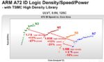
TSMC provided two charts to illustrate the PPA comparisons between these nodes.  The first depicts the comparisons for an Arm A72 core.  Recall that TSMC has focused their Foundation IP development and EDA enablement for different platforms – the comparison below utilizes the high-density based physical implementation flow associated with the Mobile and IoT platforms.

The high-performance platform (HPC) comparison for N7, N5, and N3 is shown below, using the physical implementation of the Arm A78 core as the reference.

The way to interpret these curves is that a horizontal line represents the performance gain at iso-power, which the vertical line depicts the power gains at iso-performance.

In both cases, the N7 to N5 and N5 to N3 transitions incorporate a full-node areal density increase, although it should be noted that the SRAM IP and analog density scaling factors are less.

N12e

The IoT and mobile platforms are driven by the need for ultra-low power dissipation, achieved through supply voltage reduction and the availability of ultra-low leakage (ULL, high Vt) devices.  Additionally, an ultra-low leakage SRAM bit cell offering is needed.  Also, a new class of applications – AIoT, or Artificial Intelligence of Things – is emerging for the edge-centric, ultra-low power market.

TSMC introduced a new process designation, N12e, specifically to address these requirements – working from the N12FFC+ baseline, N12e is currently in risk production status.  The N12e offering includes several key characteristics:

  • cell library IP operating at VDD = 0.4V
  • significant focus on statistical process control, to minimize device variation
  • 0.5X power (@ iso-performance) compared to N22ULL
  • 1.5X performance (@ iso-power) compared to N22ULL

The application of VDD=0.4V necessitates focus on the EDA flows for delay calculation/static timing analysis and coupled noise electrical analysis – the status of the EDA enablement for N12e will be covered in a subsequent article.   (Please refer to:  http://n12e.tsmc.com.)

RF Roadmap

To support the rapidly growing 5G market, TSMC has maintained focus on RF CMOS process development, striving for enhanced device characteristics.  The current RF offerings are based on the N28HPC and N16FFC processes.

The new RF roadmap introduced N6RF, with significantly improved power and device noise factor (NF, @5.8GHz) over current devices.   Design kit enablement for N6RF will be released in 2Q21.

Non-volatile memory (NVM) Roadmap – eFlash, RRAM, and MRAM

TSMC’s current embedded flash memory IP for the N28HPC (HKMG) node is being qualified for the automotive design platform (i.e., endurance cycles and data retention at 150C) – target date is end of 2020.

For process nodes after N28, scaling of floating gate-based flash memory becomes more difficult (expensive).  The NVM roadmap transitions to Resistive (filamentary) RAM, with N22 tapeouts this year (at 125C, non-automotive grade).  Magneto-resistive RAM (MRAM) is also available for N22 tapeouts, with automotive grade qualification in 4Q20.  Further, N16 MRAM IP will be available for risk production in 4Q21.

Initially, RRAM and MRAM technologies will be used as IP replacing eFlash applications – e.g., 10K+ endurance cycles.  TSMC indicated an “SRAM-like” MRAM IP offering for N16 will be available in 4Q22 – clearly, significant focus is being applied to increase MRAM endurance.  MRAM as a non-volatile, high-density L3/L4 SRAM-replacement memory cache will offer some very unique system architecture design opportunities.

Advanced process node fab capacity

To support the demand for nodes N16 to N5, 300mm wafer Gigafab capacity has experienced a CAGR of 28% from 2016 to 2020.  The fab capacity for N7 alone has grown 3.5X in just over two years, from 2018 to 2020.  Additionally, the capacity for N5 is planned for 3X growth from today to 2022.

Y.P. Chin highlighted that EUV learning from N7+ and N5 has enabled an extremely aggressive improvement in defect density (D0).  For example, refer to the innovation that TSMC has deployed for EUV mask cleaning:  link.

There are also major expansion plans for the Advanced Packaging line facilities in Tainan.

R&D Investment

A consistent theme through the presentations was the extensive investment TSMC is making in future technology R&D.   Specifically, TSMC is building a new R&D Center in Hsinchu, as depicted below.  The goal will be to enable “thousands of engineers” to work on new transistor architectures, materials, and process flows required for the nodes after N3, and “for the next twenty years” – more on these initiatives shortly.

Construction of the R&D center got underway in 1Q20, with occupancy starting in 2021.

Adjacent to the new R&D center, TSMC illustrated new fab construction in Hsinchu specifically designated for the “N2” process node.  Like the other TSMC Gigafabs – e.g., Fab 12, Fab 15, Fab 18, — the N2 fab construction will evolve in multiple phases.

The planned investment in R&D and fab deployment for “N2 and beyond” is definitely impressive.

Future Technology R&D

TSMC provided a glimpse into some of the future technologies currently being investigated, as the R&D activity continues to ramp.

  • RC enhancements

FinFET devices offer significant benefits in areal drive current and subthreshold leakage electrostatic channel control over planar devices – yet, one of the disadvantages is the additional Cgs and Cgd parasitic capacitance from the gate traversal over the fin(s) and the raised source/drain plus M0 metallization.  TSMC will be introducing an air-gap process in the dielectric between gate and source/drain to reduce these parasitics.

Additionally, interconnect R*C delays will be improved with the introduction of a new via trench barrier process.

  • EUV litho development

To enable aggressive lithography scaling for pitches less than 80nm using 193i illumination, TSMC introduced mask data decomposition (“coloring”) at the N20 node.  Double and quad multipatterning (SADP or 2P2E, and SAQP) have enabled further scaling.   Inverse lithography technology (ILT) algorithms, as part of a source-mask optimization (SMO) mask data preparation methodology, was also deployed.   13.5nm EUV lithography was introduced for N7+, as mentioned above.  To enable further scaling, EUV multipatterning (2P2E) is required.

TSMC showed lithographic patterning/etch in support of an 18nm interconnect pitch.

  • high NA EUV

The numerical aperture of a lithography system defines the resolution capability, a function of the cone of light captured  and the refractive index of the entire lens system.  The resolution is inversely proportional to the NA.  TSMC is working closely with ASML on the next generation of “high NA” EUV equipment and corresponding resist technology, to enable finer resolution in future nodes.

  • GAA nanosheets

TSMC highlighted their R&D efforts to implement gate all-around nanosheets, as a FinFET replacement.

The N3 process definition starts with a conventional FinFET device.  (To achieve increased performance and fin pitch, the fin height and aspect ratio for N3 will need to be improved.)

As has been the case for TSMC node transitions, adhering to the roadmap schedule has been a paramount priority.  Y.J. Mii said, “After carefully evaluating customer needs and technology maturity, N3 continues to use FinFET devices.  Our R&D team has extensive experience with nanowire and nanosheet technology, and have demonstrated 32Mb SRAM testsite yield.  We will have the technology options for each new node ready in advance – the right technology at the right time.”  It will be interesting to see how GAA device architectures evolve.

  • unique “2D” device semiconducting channel material

TSMC referred to a technical paper published earlier this year, showing promising results for a replacement to the Si (or SiGe) FinFET device.  Semiconducting “monolayers” of MoS2 serve as the (planar) field-effect device channel, offering improved carrier mobility.  (Reference:  A.S. Chou, et al., VLSI Symposium 2020).

The figure below illustrates a single monolayer of MoS2, the HfO2 gate dielectric, and either a (large area) Si or a local Pt “back gate” device structure.  The device drive current and Ion/Ioff ratio shows great promise – reducing the contact resistance (Rc) from the S/D metal to the semiconducting layer is a key process development challenge.

  • carbon nanotubes

TSMC also referred to a recently published paper illustrating the implementation of a deposited layer of carbon nanotubes (CNT) for a unique application.  The nanotubes were incorporated as part of the (low temperature-restricted) back-end-of-line flow in N28, with patterning of gate and source/drain metallization.  The specific application for which these devices are targeted is for the logic circuit power-gating “header”.  (Reference:  Cheng, et al, IEDM, 2019, paper 19.2)

Current power-gating implementations utilize multiple silicon devices (low R) connected between the “always on” and switched power rails connected to the block logic.  These designs require unique block-level physical design, specific cell library images, and modified (global/local) power distribution networks, adversely impacting areal circuit density and routability.  A semiconducting CNT power gating circuit could offer a significant PPA boost – ongoing focus on reducing the overall series “on” resistance will be key.

As an aside, it is perhaps unwise to read too much into the R&D part of the Symposium presentations, in terms of what was and was not mentioned for post-N3 architectures.  Nevertheless, the following options being widely investigated within the semiconductor industry were not discussed:  negative-capacitance FETs (NC-FETs, integrating ferroelectric materials), vertical nanowires (VNW), tunnel FETs, or N3XT (“full 3D” die integration of logic, memory, and NVM).

Look for subsequent articles highlighting TSMC packaging technology and design enablement presentations to follow.

-chipguy

Highlights of the TSMC Technology Symposium – Part 2

Highlights of the TSMC Technology Symposium – Part 3


How an Nvidia/ARM deal could create the dominant ecosystem for the next computer era

How an Nvidia/ARM deal could create the dominant ecosystem for the next computer era
by Michael Bruck on 09-04-2020 at 6:00 am

PC operating profits

Over the past few weeks, there have been numerous reports about Nvidia’s overtures to acquire Arm. The news has mostly been obsessed about the $31 billion that Arm’s current owner, Softbank, paid for Arm and whether Nvidia could pay such an eye-watering price to buy this asset. There is also pushback from Herman Hauser who was one of Arm’s earliest backers, raising concerns that Arm’s destiny is vital for Britain’s future, which is an odd concern given that Softbank is a Japanese company. Putting all this aside for a moment, I would like to focus on the strategic importance of such a merger and, if the merger does go through, why this could result in a momentous change in the balance of power in the computer and semiconductor industry and why a combined Nvidia and Arm could truly be a game-changer.

The next strategic inflection point in computing will be the cloud expanding to the edge, involving highly parallel computer architectures connected to hundreds of billions of IoT devices. Nvidia is uniquely positioned to dominate that ecosystem, and if it does indeed acquire ARM within the next few weeks as expected, full control of the ARM architecture will virtually guarantee its dominance.

Every 15 years, the computer industry goes through a strategic inflection point, or as Jefferies US semiconductors analyst Mark Lipacis calls it, a tectonic shift, that dramatically transforms the computing model and realigns the leadership of the industry. In the ’70s the industry shifted from mainframe computers, in which IBM was the dominant company, to minicomputers, which DEC (Digital Equipment Corporation) dominated. In the mid-’80s the tectonic shift was PCs, where Intel and Microsoft defined and controlled the ecosystem. Around the turn of the millennium, the industry shifted again to a cell phone and cloud computing model; Apple, Samsung, TSMC, and ARM benefited the most on the phone side, while Intel remained the major beneficiary of the move to cloud data centers. As the chart below shows, Intel and Microsoft (a.k.a. “Wintel”) were able to extract the majority of the operating profits in the PC era.

Source: Jefferies, company data

According to research from investment bank Jefferies, in each previous ecosystem, the dominant players have accounted for 80% of the profits. For example, Wintel in the PC era and Apple in the smartphone era. These ecosystems did not happen by accident and are the result of a multi-pronged strategy by each company that dominated its respective era. Intel invested vast sums of money and resources into developer support programs, large developer conferences, software technologies, VC investments through Intel Capital, marketing support, and more. The result of the Wintel duopoly can be seen in the chart above. Apple has done much the same, with its annual developer conference, development tools, and financial incentives. In the case of the iPhone, the App Store has played an additional role, making the product so successful, in fact, that it is now the target of complaints by the developers who played a key role in cementing Apple’s dominance of the smartphone ecosystem. The chart below shows how Apple has the lion’s share of the operating profits in mobile phones.

Source: Jefferies, company data

Intel maintained dominance of the data center market for decades, but that dominance is now under threat for several reasons. One is that the type of software workload mobile devices generate is changing. The vast amounts of data these phones generate requires a more parallel computational approach, and Intel’s CPUs are designed for single-threaded applications. Starting 10 years ago, Nvidia adapted its GPU (graphics processing unit) architecture (originally designed as a graphics accelerator for 3D games) into a more general-purpose parallel processing engine. Another reason Intel is under threat is that the much larger volume of chips sold in the phone market has given TSMC a competitive advantage, since TSMC was able to take advantage of the learning curve to get ahead of Intel in process technology. Intel’s 7nm process node is now over a year behind schedule. Meanwhile, TSMC has shipped over a billion chips on its 7nm process, is getting good yields on 5nm, and is sampling 3nm parts. Nvidia, AMD, and other Intel competitors  are all manufacturing their chips at TSMC, which gives them a major competitive advantage.

Nvidia’s domain

Parallel computing concepts are not new and have been part of computer science for decades, but they were originally relegated to highly specialized tasks such as using supercomputers to simulate nuclear bombs or weather forecasting. Programming parallel processing software was very difficult. This all changed with the CUDA software platform that Nvidia launched 13 years ago and which is now on its 11th generation. Nvidia’s proprietary CUDA software platform lets developers leverage the parallel architecture of Nvidia’s GPUs for a wide range of tasks. Nvidia also seeded computer science departments at universities with GPUs and CUDA, and over many iterative improvements the technology has evolved into the leading platform for parallel computing at scale. This has caused a tectonic shift in the AI industry — moving it from a “knowledge-based” to “data-based” discipline, which we see in the growing number of AI-powered applications. When you say “Alexa” or “Hey Siri,” the speech recognition is being processed and interpreted by a parallel processing software algorithm most likely powered by an Nvidia GPU.

A leading indicator for computer architecture usage is Cloud Data Instances. The number of these instances represents the usage demand for applications in the leading CSPs (cloud service providers), such as Amazon AWS, Google Cloud Platform, Microsoft Azure, and Alibaba Cloud. The top four CSPs are showing that Intel’s CPU market share is staying flat to down, with AMD growing quickly, and ARM with Graviton getting some traction. What is very telling is that demand for dedicated accelerators is very strong and being dominated by Nvidia.

Source: Jefferies, company data

Nearly half of Nvidia’s sales revenues are now driven by data centers, as the chart above shows. As of June this year, Nvidia’s dedicated accelerator share in cloud data instances is 87%. Nvidia’s accelerators have accounted for most of the data center processor revenue growth for the past year.

The company has created a hardware-software ecosystem comparable to Wintel, but in accelerators. It has reaped the rewards of the superior performance of its architecture and of creating the highly popular CUDA software platform, with a sophisticated and highly competitive developer tools and ecosystem support program, a highly attended annual GPU Technology Conference, and even an active investment program, Inception GPU Ventures.

Where ARM comes in

But Nvidia has one competitive barrier remaining that prevents it from complete domination of the data center ecosystem: It has to interoperate within the Wintel ecosystem because the CPU architecture in data centers is still x86, whether from Intel or AMD.

ARM’s server chips market share is still minute, but it has been extremely successful. And, with TSMC as a manufacturing partner, it is rapidly overtaking Intel in raw performance in market segments outside of mobile phones. But ARM’s weakness is that the hardware-software ecosystem is fragmented, with Apple and Amazon having a mostly proprietary software approach and smaller companies such as Ampere and Cavium being too small to create a large industry ecosystem comparable to Wintel.

Nvidia and ARM announced in June that they will work together to make ARM CPUs work with Nvidia accelerators. First of all, this collaboration gives Nvidia the ability to add computing capabilities to its data center business. Secondly, and more importantly, it puts Nvidia in a strong position to create a hardware-software ecosystem around ARM that would be a serious threat to Intel.

The coming shift

The reason such a partnership is particularly important today is because the computer industry is going through its next strategic inflection point. This new tectonic shift will have major repercussions for the industry and the competitive landscape. And if historical trends continue, a merged Nvidia/ARM would result in a market at least 10 times larger than today’s mobile phone or cloud computing market. It is an understatement to say that the stakes are huge.

There are several forces driving this new shift. One is the emergence of faster 5G networks that are designed to support a far larger number of devices. One of the key features of 5G networks is edge computing, which will put high-performance computing right at the very edge of the network, one hop away from the end-device. Today’s mobile phones are still tied to a descendant of the old client-server architecture established in the ’90s with networked PCs. That legacy results in high latency networks, which is why we experience those annoying delays on video calls.

Next-generation networks will have high-performance computers with parallel accelerators at the very edge of the network. The endpoints — including autonomous vehicles, industrial robots, 3D or holographic communications, and smart sensors everywhere — will require a much tighter integration with new protocols and software architectures. This will achieve much faster, and extremely low latency communications through a distributed computing architecture model. The amounts of data produced — and needing processing — will increase by orders of magnitude, driving demand for parallel computing even further.

Nvidia’s roadmap

Nvidia has already made its intentions clear that cloud-to-edge computing is on its roadmap:

“AI is erupting at the edge. AI and cloud native applications, IoT and its billions of sensors, and 5G networking now make large-scale AI at the edge possible. But it needs a scalable, accelerated platform that can drive decisions in real time and allow every industry to deliver automated intelligence to the point of action — stores, manufacturing, hospitals, smart cities. That brings people, businesses, and accelerated services together, and that makes the world a smaller, more connected place.”

Last year Nvidia also announced that it is working with Microsoft to collaborate on the Intelligent Edge.

This is why it makes strategic sense for Nvidia to buy ARM and why it would pay a very high price to be able to own this technology. Ownership of ARM would give Nvidia greater control over every aspect of its ecosystem with far greater control of its destiny. It would also eliminate Nvidia’s dependence on the Intel compute stack ecosystem, which would greatly increase its competitive position. By owning ARM instead of just licensing it, Nvidia could add special instructions to create even tighter integration with its GPUs. To get the highest performance, one needs to integrate the CPU and GPU on one chip, and since Intel is developing its competing Xe line of accelerators, Nvidia needs to have its own CPU.

Today Nvidia leads in highly parallel compute and Intel is trying to play catch-up with its Xe lineup. But as we have learned from the PC Wintel days, the company that controls the ecosystem has a tremendous strategic advantage, and Nvidia is executing well to position it to become the company that will be the dominant player in the next era of computing. Nvidia has a proven track record of creating an impressive ecosystem around its GPUs, which puts it in a very competitive position to create a complete ecosystem for edge computing including the CPU.

Michael Bruck is a Partner at Sparq Capital. He previously worked at Intel, where he was Chief of Staff to the then CEO, Andy Grove, before heading Intel’s business in China.


World’s Leading Chip Designers at IDEAS Digital Forum Show How to Streamline Design Flows and Reduce Design Cost

World’s Leading Chip Designers at IDEAS Digital Forum Show How to Streamline Design Flows and Reduce Design Cost
by Daniel Nenni on 09-03-2020 at 10:00 am

ANSYS IDEAS Airplane

Innovative Designs Enabled by Ansys Semiconductor

I’m excited to announce that general registration is now open for the new Ansys IDEAS Digital Forum!  IDEAS, hosted by Ansys Semiconductor, is a virtual gathering of top industry executives, thought leaders, and designers from some of the biggest IP, chip design, semiconductor foundry and electronic system companies in the world. Log in to IDEAS to join with your peers to listen to industry leaders and technical experts discuss the semiconductor industry. And then ask them questions in live Q&A sessions.

Design automation and multiphysics simulation tools are key leverage points in your production flow where you have options available to not only reduce your risk profile but also influence the bottom line by reducing costs, improving product quality, and speeding time to market.  IDEAS is an opportunity for you to stay on top of what is going on in the electronic design market with Keynote presentations from senior industry executives including:

  • Len Orlando III Air Force Research Laboratory Sensors Directorate, Wright Patterson AFB
  • Prith Banerjee CTO, Ansys
  • Rob Aitken R&D Fellow, ARM
  • Vicki Mitchell & Rob Harrison VP of Engineering & Sr. Director at ARM
  • Dhiraj Mallick VP of Engineering at Cerebras Systems
  • Eric Ladizinsky Co-Founder and Sr. Scientist at D-Wave Systems
  • Mallik Tatipamula CTO of Ericsson SV
  • Subhasish Mitra of Electrical Engineering and Computer Science, Stanford University
  • Suk Lee Sr. Director of Design Infrastructure Marketing at TSMC

These distinguished, high profile executives will be sharing their insights on technology and business trends from multiple perspectives and will be taking live questions from audience members attending IDEAS.

The theme of IDEAS Digital Forum focuses on how multiphysics simulation is accelerating the twin industry trends of Moore and Beyond Moore. Moore’s Law is racing towards ever smaller silicon process geometries, with 3nm now on the horizon. This enables huge ICs to be designed for AI/ML applications, high-performance computing, and 5G. But the expense of designing at the leading edge is also rising and a second evolutionary path has emerged called Beyond Moore, or More Than Moore,  that pushes a parallel evolutionary track based on a multi-die approach to system integration with technologies like 3DIC, wafer-scale integration, and a disaggregation of SoCs into discrete chiplets for applications ranging from intelligent sensors, autonomous, and edge-node compute.  It is a fascinating time to be in semiconductors with these complex market and technology forces creating many opportunities and tradeoffs on which approach to pick, based on your end application.

The afternoons of both days at IDEAS are taken up with technical Breakout Sessions featuring over 30 speakers from companies including:

Intel Nvidia Qualcomm
Broadcom MediaTek ST Microelectronics
Samsung Alphawave Synaptics
Google HP Enterprise Xilinx

These sessions will focus on practical design experiences for applications in the areas of 3D-IC electrothermal analysis, electromagnetic coupling, the timing impact of voltage drop, RTL power analysis, and power integrity signoff.  Here too, virtual attendees logged in to IDEAS will be able to submit questions to the authors in real time and get immediate answers.

For a broader perspective, the Multiphysics Solutions track will feature experts on industry-wide technology challenges including 5G communications, autonomous vehicles, designing in the cloud, and design for  reliability. They will highlight how electronic design is impacted by these larger industry drivers and the particular challenges they pose.

Please join us and your industry colleagues in exploring the latest in electronic design at IDEAS by registering at www.ansys.com/ideas – and see what’s ahead.

Also Read

Ansys Multiphysics Platform Tackles Power Management ICs

Qualcomm on Power Estimation, Optimizing for Gaming on Mobile GPUs

The Largest Engineering Simulation Virtual Event in the World!


Cerebras and Analog Bits at TSMC OIP – Collaboration on the Largest and Most Powerful AI Chip in the World

Cerebras and Analog Bits at TSMC OIP – Collaboration on the Largest and Most Powerful AI Chip in the World
by Mike Gianfagna on 09-03-2020 at 6:00 am

Cerebras Wafer Scale Engine

This is another installment covering TSMC’s very popular Open Innovation Platform event (OIP), held on August 25. This event presents a diverse and high-impact series of presentations describing how TSMC’s vast ecosystem collaborates with each other and with TSMC. The topic at hand was full of superlatives, which isn’t surprising when Cerebras and Analog Bits talk about  how they effect collaboration on the largest and most powerful AI chip in the world.  

The presentation began with Dhiraj Mallick. vice president engineering and business development at Cerebras Systems. Dhiraj introduced Cerebras as an exciting AI systems startup with a mission to transform the landscape of compute by accelerating a new class of workloads like AI orders of magnitude over today’s state-of-the-art. Dhiraj discussed the challenges of tasks such as deep learning training. He explained that compute requirements for these types of workloads have increased 300,000-fold over the past eight years. This equates to a doubling every 3.4 months. Those who follow Moore’s Law will realize how significant this acceleration is.

To address this problem, Cerebras has built the world’s largest processor. The statistics of this chip, pictured above, are mind-boggling. The chip is over 46,000 mm2 in size, equivalent to about 60 reticle-limited chips. It contains 400,000 cores, all fully programmable and optimized for deep learning and sparse linear algebra. The chip contains 18 GB on-chip SRAM with unprecedented memory bandwidth and a mesh system for core-to-core communication capable of 100 Pb/s. When you are collaborating on the largest and most powerful AI chip in the world, everything is record-breaking.

Dihraj went on to discuss the challenges of power integrity with a design like this. He explained that hundreds of thousands of independent cores on a single piece of silicon result in dynamic current surges causing die voltages to exceed functional limits. System performance consequences can include catastrophic failures. The approach Cerebras chose to address this challenge was to use an analog glitch detection circuit from Analog Bits. These devices have a real-time response and 840 of them were distributed over the Cerbras wafer-scale chip. Dihraj explained a significant advantage of the Analog Bits IP was its ability to detect anomalies with much higher bandwidth than digital approaches, resulting in true real-time identification of power integrity events. The benefits of the Analog Bits solution can be summarized as follows:

  • High-precision, real-time power supply monitoring IP exceeding 5pVs sensitivity
  • Fully integrated analog macro that interfaces to a digital SoC environment
  • Highly user programmable for trigger voltages, depth of glitch, time-span of glitches
  • The ability to monitor multiple thresholds simultaneously, providing a wealth of data to optimize the instantaneous current spike suppression and overall effectiveness

Dihraj then introduced Mahesh Tirupattur, executive vice president at Analog Bits to cover more details about Analog Bits IP and collaboration with TSMC. Mahesh began with an overview of the various Analog Bits IP that address clocking, I/O, sensing and serial communication. He explained that Analog Bits takes a system view of problem solving. The figure below summarizes their offerings.

Mahesh then focused on the company’s sensor technology. Their on-die PVT sensor monitors voltage, temperature and process in one block. An integrated power on reset monitor is also available, as well as a power supply glitch detector. This last block was developed in collaboration with their customers, including Cerebras. It measures voltage spikes as well as voltage drops. This block has some unique features, as summarized below:

  • Integrated voltage reference for precision stand-alone operation
  • Easy to integrate with no additional components or special power requirements
  • Easy to use and configure
  • Cascadable for up to 4 additional glitch detection channels
  • Independent programming available for glitch detection levels
  • Low power
  • Implemented with Analog Bits’ proprietary architecture
  • Requires no additional on-chip macros, minimizing power consumption

Mahesh then elaborated on more of the unique capabilities of the glitch detector IP. He then provided silicon results of five corner lots at extreme voltage conditions, both trimmed and untrimmed. Regarding the roadmap, the glitch detector IP is silicon-proven in TSMC’s 7FF process, with N5 available in Q3-2020 and N3 available in Q1-2021. In addition, Analog Bits is working on a system power supply detection macro in TSMC N5. This IP provides synchronous detection with latched outputs. It also offers a programmable droop detection level. It will be available in Q3-2020.

Mahesh closed with some comments about the collaboration between TSMC and Analog Bits, which dates back to 2004. Several test chips have been done as a result of this collaboration. He described an N7 test chip done last year that included 5 corner split lots, with exhaustive characterization reports available and IP 9000 certification. Mahesh concluded with some corporate background on Analog Bits, as summarized below. The collaboration between Cerebras and Analog Bits to create the largest and most powerful AI chip in the world was quite impressive. To learn more, visit the Analog Bits website.

Also Read:

AI processing requirements reveal weaknesses in current methods

7nm SERDES Design and Qualification Challenges!

CEO Interview: Alan Rogers of Analog Bits


Lip-Bu Hyperscaler Cast Kicks off CadenceLIVE

Lip-Bu Hyperscaler Cast Kicks off CadenceLIVE
by Bernard Murphy on 09-02-2020 at 6:00 am

Lip Bu min

Lip-Bu (Cadence CEO) sure knows how to draw a crowd. For the opening keynote in CadenceLIVE (Americas) this year, he reprised his data-centric revolution pitch, followed by a talk from a VP at AWS on bending the curve in chip development. And that was followed by a talk by a Facebook director of strategy and technology on aspects of their hardware strategy. CadenceLIVE: Lip-Bu+hyperscaler cast, all delivered in 60 minutes. Not bad.

Lip-Bu on Cadence

The Cadence top-level story remains very consistent. Data in one way or another is driving every aspect of innovation: In compute, in storage, in networking and in analytics. Some of the obvious trends in compute are application-driven system design. Witness Amazon, Google, Facebook, Baidu, TenCent and many others building their own hardware. Some design is very domain-specific, in AI accelerators, for example. Systems companies are also contributing to innovation in storage (Facebook was very instrumental in driving NVMe data caching) and in networking: Reconfigurable options for on-the-fly virtualization optimization. There’s plenty of basic innovation as well. Networking bandwidths soaring towards 50 Tbps and all kinds of new warm to hot memory technologies: Phase-change, magnetic, quasi-volatile and others.

Cadence’s role in supporting this explosion of new technology continues with the theme Intelligent System Design. “Design” encompasses the core design technologies: IP, functional verification, digital IC design and signoff, custom design and simulation. “System” is system interconnect (Allegro, not just for PCB, also packaging and 3D). Then implementation analytics and high speed RF design (this is new, I’ll talk more in my next CadenceLIVE blog), also system and embedded software partnerships, leveraging the Green Hills relationship. “Intelligent” applies AI and machine learning for further optimization. Consistent direction with incremental growth around system implementation and analytics and growth into secure embedded software and RF.

Nafea Bshara on design at AWS

Nafea co-founded Annapurna Labs, subsequently acquired into Amazon/AWS. These are the folks who developed the Arm-based AWS Graviton processor follow-ons, now available in the AWS cloud. Graviton makes headlines, they’re also working on AWS Inferentia for machine learning / inference and AWS Nitro for cloud hypervisor, network, storage and security.

Good stuff, but I was especially interested in his views on the benefits of design in the cloud. I wrote another blog on this topic recently, arguing that established cloud use in other departments in a design enterprise—finance, HR, legal—together with security and liability concerns, all tilt the scale towards cloud-centric use. All valid arguments but they don’t speak to many designers who aren’t directly involved in financial and legal concerns. Nafea talked about engineering concerns. Nafea’s group switched from their own datacenter to the cloud when they moved to 16nm. Yeah, they’re in AWS, but they’re still measured on design deliverables. They wouldn’t have switched if doing so didn’t accelerate meeting their goals.

The benefit of the cloud in engineering terms

Nafea talked about the relative predictability in compute demand which allows a design team to take advantage of spot pricing for much of their activity, still allowing to surge above that level as needed at demand-based pricing. When you’re done, or when you return to low-level needs as you forecast, you’re not paying for what you don’t need.

He contrasted that with the classical datacenter update approach. Periodic cross-group debates on what everyone wants, all different of course. Some high-end servers versus masses of mid-range servers, lots of cold-storage disks versus tradeoff with NVMe warm storage. Support for fast remote site access and demand. You wrestle and wrangle, wind up with some kind of compromise, which, at a big price tag, fails to completely satisfy anyone. Nafea contrasted with the cloud approach. Every design manager gets a budget to use however they choose. They buy access to whatever they want with the latest and greatest options the cloud provider has offer, if necessary, or many lower-priced servers for bulk regressions if that’s what they need, unconstrained by other department needs. Each design manager has complete control over how they manage their workload. That is a pretty compelling engineering motivation to switch.

Vijay Rao on hardware infrastructure at Facebook

Vijay talked about datacenter challenges at Facebook. A lot of this was on the very top-level facilities aspects of datacenters, construction, power distribution, cooling, that sort of thing. Fascinating stuff, though not directly relevant to much of my audience. I’ll call out a few things that struck me. We all know that Facebook hosts huge traffic—billions of users on Facebook, Messenger, Instagram and WhatsApp. Traffic that can be pretty spiky around holidays and major world crises. Much of this is high data volume— image/video upload, web-serving, video chats. Thanks to many more of us working from homes now, demand is spiking to unprecedented levels. Managing all this traffic with a continued strong user experience places extraordinary demands on the hardware. Which, incidentally, is why Facebook is a leader in initiatives like NVMe and the Telecom Infra Project.

Vijay talked particularly about their AI development at Facebook. They use AI for bots in Messenger to generate video trailers, to enable VR and AR, to run translations between languages. They use AI to catch policy violations (a sensitive topic these days). He talked about their development on a common compute platform for compute and AI inference. They share this work through the OpenCompute project, an organization they founded in 2011, which is now supported by all the big names in technology certainly, but far beyond as well (Shell and Goldman Sachs for example). Lots of leading-edge high volume and high-performance demand.

A fascinating kickoff to CadenceLIVE 2020. Check HERE for more on Intelligent System Design.

Also Read

Quick Error Detection. Innovation in Verification

The Big Three Weigh in on Emulation Best Practices

Cadence Increases Verification Efficiency up to 5X with Xcelium ML


WEBINAR: Addressing Verification Challenges in the Development of Optimized SRAM Solutions with surecore and Mentor Solido

WEBINAR: Addressing Verification Challenges in the Development of Optimized SRAM Solutions with surecore and Mentor Solido
by Daniel Nenni on 09-01-2020 at 2:00 pm

surecore solido webinar graphic

After spending a significant amount of my career in the IP library business it was an easy transition to Solido Design. I spent 10+ years traveling the world with CEO Amit Gupta working with the foundries and their top customers. In fact, the top 40 semiconductor companies use Solido. IP companies are also big Solido users including custom SRAM maker sureCore.

In my experience the best EDA and IP information comes from users and that is the basis for this webinar. surecore is a long time user of Solido tools and presents some case studies based on that usage. I learned a lot preparing for this webinar and it was great to reconnect with Amit and Tony, two highly regarded experts in this field.

Bottom line: If you have SRAM in your low power design this is a must attend event, absolutely.

Registration here and get the replay if you cannot attend.

Addressing Verification Challenges in the Development of Optimized SRAM Solutions

On-chip memory makes up an increasingly large proportion of the area of modern SoCs, and consequently optimising memory IP to match the specific requirements of an application is a way to improve the power, performance and area (PPA) metrics of new SoCs.

In several recent customer projects SureCore has demonstrated significant improvements in area, speed, and/or power by combining customer application knowledge with SureCore’s memory expertise. Statistical verification is a critical feature of the development flow and exploiting the Solido tool suite enables a rapid exploration of parts of the design space that are otherwise hard to quantify.

In this webinar SureCore and Solido will explain how they have been able to deliver dramatic PPA improvements while ensuring design reliability.

SPEAKERS:
TONY STANSFIELD, CHIEF TECHNOLOGY OFFICER, SURECORE
Tony has over 35 years of semiconductor industry experience in a variety of technical roles. He started his career with the Inmos UK Memory and Graphics group, where he designed SRAMs and Caches for multiple Inmos products. He later joined HP Labs to work on high-speed programmable imaging datapaths, and was a co-founder and VP Hardware Architecture at Elixent, the company created to deliver custom Silicon IP based on that technology. Following the acquisition of Elixent by Panasonic, he was a key member of the team that integrated this technology into multiple generations of TV chipsets. Tony is cited as an inventor on 23 patents covering SRAM, CAM, low-power electronics, and programmable logic.

AMIT GUPTA, GM, MENTOR IC VERIFICATION SOLUTIONS SOLIDO
Amit is General Manager of the IC Verification Solutions Solido division of Mentor, a Siemens Business. Previously, he founded Solido Design Automation Inc. in 2005 and served as its President and CEO until its acquisition by Mentor in 2017. Solido is a leader in machine learning variation-aware design and characterization.

About sureCore Limited
sureCore is the Low Power leader that empowers the IC design community to meet their aggressive power budgets through a portfolio of innovative, ultra-low power memory design services and standard products. sureCore’s low-power engineering methodologies and design flows helps you meet your most exacting memory requirements with customized low power SRAM IP and low power mixed signal design services that create clear marketing differentiation. The company’s low-power product line encompasses a range of down to near-threshold silicon proven, process-independent SRAM IP.

Also Read:

Low Power Design – Art vs. Science

WEBINAR: The Brave New World of Customized Memory

Custom SRAM IP @56thDAC


Webinar: Maximize Performance Using FPGAs with PCIe Gen5 Interfaces

Webinar: Maximize Performance Using FPGAs with PCIe Gen5 Interfaces
by Mike Gianfagna on 09-01-2020 at 10:00 am

Maximize Maximize Performance Using FPGAs with PCIe Gen5 Interfaces

FPGAs are a popular method to implement hardware accelerators for applications such as AI/ML, SmartNICs and storage acceleration. PCIe Gen5 is a high bandwidth communication protocol that is a key enabler for this class of applications. Putting all this together presents significant demands on the FPGA for performance and throughput. I had the opportunity to preview an upcoming webinar on this topic presented by Achronix. The specialized approach taken by the Achronix flattens many very difficult problems. They are truly able to maximize performance using FPGAs with PCIe Gen5 interfaces. I’ll provide some background on the webinar to whet your appetite. Stay tuned for the registration link, you’ll want to watch this one.

First, a bit about Achronix. They are an FPGA/embedded FPGA vendor that focuses on specialized, high performance architectures. Their Speedster7t FPGA family is optimized for high-bandwidth workloads and eliminates the performance bottlenecks associated with traditional FPGAs. The product family is built on TSMC’s 7nm FinFET process. You can learn more about the company from an interview Dan Nenni did with Robert Blake, the CEO of Achronix.

The webinar is presented by Kent Orthner, senior director, systems at Achronix. Kent has an easy to follow presentation style. He packs a lot of information into a webinar that’s only about 30 minutes long. Kent has a long history of hardware and software engineering leadership at Arteris and Altera, so he definitely inspires confidence.

To finish setting the stage, let’s take a look at PCIe Gen5. This protocol represents the latest performance level in a long history of this standard as shown in the figure below. This latest version also supports more embedded signal integrity technology features. Protocols such as Compute Express Link (CXL) and NVMe are built on the PCIe Gen5 physical layer specification. Gen 5 will continue to be backward compatible with prior versions and wide deployment in data center and networking applications is expected.

So, what is discussed about maximizing performance using FPGAs with PCIe Gen5 interfaces and why is it so important? The webinar goes into the details of three application areas, as summarized below.

  • Compute acceleration – AI/ML seeing exponential increase
    • AI applications, like autonomous vehicles, generate 4TB data per day
    • AI/ML training models doubling in size every 3-4 months
    • Enterprise workloads moving to cloud, accelerated by increasing number of workers from home
    • CPUs can’t keep up; need heterogeneous compute with specialized acceleration hardware
  • SmartNIC
    • A network interface card (network adapter) that offloads processing tasks that the system CPU would otherwise handle
    • SmartNIC performs any combination of encryption/decryption, firewall, TCP/IP, SDN, etc.
  • Storage acceleration
    • Using specialized hardware to reduce CPU load, and to improve throughput and latency to non-volatile storage devices such as hard drive arrays and flash memory.
    • g., inline compression, encryption and hashing, erasure coding, deduplication, string/image search, database operations e.g., sort/join/filter

For each of these areas the challenges of using standard FPGAs as hardware accelerators are described. The details of the unique features of the Achronix architecture to address these challenges are also presented. You’ll have to watch the webinar for the whole story, but here are some bits of information: Special FPGA enhancements such as a custom-designed, configurable on-chip network system offloads the FPGA fabric and delivers high performance and low latency. This system also simplifies timing closure and floor planning.  There is also an array of math blocks optimized for AI/ML as well as support for high-speed SerDes, 400G Ethernet, GDDR6 and, of course support for PCIe Gen 5.

The webinar presents three real applications of the technology:

  • Data center acceleration – machine learning inference
  • 400 Gbps SmartNiC
  • Storage acceleration

The details and results presented for these three scenarios are substantial and impressive. You will truly learn how to maximize performance using FPGAs. There’s sure to be something in there that will get your attention. The webinar will be presented on Tuesday, September 15, 2020 at 10AM PDTYou can register for the webinar here.


Creating Analog PLL IP for TSMC 5nm and 3nm

Creating Analog PLL IP for TSMC 5nm and 3nm
by Tom Simon on 09-01-2020 at 6:00 am

PLL Optimizations

TSMC’s Open Innovation Platform’s main objective is to create and promote partnership for producing chips. This year’s OIP event included a presentation on the joint efforts of Silicon Creations, Mentor, a Siemens business and TSMC to produce essential PLL IP for 5nm and 3nm designs. The relentless push for smaller geometries has created huge challenges for all kinds of designs but have pushed analog blocks further than ever. Mentor and Silicon Creations presented the results for 5nm and 3nm PLLs, which are critical IP for any digital or analog design. In particular large high speed SoCs live or die on PLL performance.

PLLs are some of the highest volume analog IPs. Silicon Creations’ PLL TS28HMP FRAC is used on 140 different production chips accounting for an incredible instance count of over one billion. Achieving the reliability necessary for those volumes while meeting increasingly tighter specifications and with the compounding difficulties of shrinking process geometry is no small feat.

PLL Optimizations

No matter how good Silicon Creations’ design team is, they simply could not get their widely used IP out the door without the efforts of Mentor and TSMC. Mentor has contributed to this success with their innovative Analog FastSPICE (AFS) Platform. TSMC, in addition to their advanced fabrication capabilities, provide silicon accurate models for cells, devices and interconnect.

I have written previously about Silicon Creations’ advanced process node IP as they were heading into 5nm. They reported first pass silicon success at 5nm and several active projects in flight for 3nm. Silicon Creations has been TSMC’s Mixed Signal Partner of the Year from 2017 to 2019.

So, what are the specific challenges that come with moving further along from 5nm to 3nm? The number of GDS layers needed has increased 9X since 180nm. The Design Rule Manual has increased an order of magnitude from 180nm to 3nm. Consequently, DRC runs are now 100X longer at 5nm than at 180nm. So, clearly process complexity is a real issue.

Well, does analog scale in a way anything like digital? According to the presentation, it does scale, but not nearly as handily as digital. Expect to see a 10X reduction in area compared to the 1000X seen in digital in going from 180nm to 3nm. In looking at the graph provided it looks like there is a local minimum around 7nm, so the future of scaling will be interesting to see.

The real fly in the ointment is interconnect, which is becoming an extremely important limiting factor for analog designs at 3nm. From 40nm to 3nm relative wire resistance (Ohms/sq) has risen almost an order of magnitude. TSMC is working to relieve the pressure on designers, but the issue will never entirely go away. Now, even early functional verification simulations need to account for parasitics. This is pushing simulation times up at an incredible rate. The effects of this include longer development cycles and the need for more simulation licenses. The presentation offers some hope through the effective RC reduction found in AFS.

Another source of pain for simulation is the large range of time scales that must be looked at to verify a design. From the ~100fs scale of jitter requirements to the ~1ms time required to analyze link requirements, the scope of timeframes ranges almost 10 orders of magnitude. Also, many analog subsystems require extensive simulation to ensure proper operation. Some examples that were provided include digital spread spectrum modulation, digital jitter cleaner, fast hopping FLL for DFS, phase alignment, and fractional LC PLL with noise cancellation.

Silicon Creations talked about how they rely on the many advanced features of Mentor’s AFS Platform to get through the simulation process. They report that they see good correlation with AFS and silicon measurement. They included graphs comparing simulation and silicon measurements for phase noise at 5nm, IoT PLL fast locking, oscillator frequency stability and transient noise.

The papers at TSMC’s OIP event are usually pretty comprehensive and interesting. This one was no exception. It also goes into detail on the Silicon Creations compute farm, PLL applications, and several other aspects of their verification flow. There is interesting detail about the complete AFS platform as well. I highly suggest viewing the presentation replay.

Also Read:

Essential Analog IP for 7nm and 5nm at TSMC OIP

Keeping Pace With 5nm Heartbeat

Context is Everything – especially for autonomous vehicle IP