webinar banner AI 2026 v2

Tesla’s Musk Mocks Marketing

Tesla’s Musk Mocks Marketing
by Roger C. Lanctot on 12-27-2020 at 10:00 am

Teslas Musk Mocks Marketing

The Automotive News had a standout year in 2020 – thriving at a time when many publishers suffered. With factories and dealerships shuttered in the spring due to the pandemic, the outlook was bleak but the Automotive News dug in amplifying its reporting with multiple podcasts and video content documenting the ups and downs of the industry recovery.

Nowhere was this community service and news amplification more focused than in the Daily Drive podcast where Automotive News Publisher Jason Stein and fellow editors and reporters recorded interviews with industry notables describing their day-to-day experiences and pandemic responses. Paired with the Shift Automotive podcasts, Automotive News pumped out hundreds of these enlightening segments – all freely accessible for listeners stuck at home or needing background noise for a socially distanced workout.

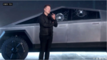
The best of these podcasts, bar none, was Jason Stein’s exclusive interview with Tesla Motors’ CEO Elon Musk. And the moment that crystalizes the events of 2020 and Tesla’s and Musk’s role in the industry comes at 8:20 of the latest condensation of that interview where Stein asks Musk if Tesla did any customer research when designing its upcoming Cybertruck.

Condensed Stein-Musk interview from Automotive News “Daily Drive” podcast:   https://www.autonews.com/weekend-drive-podcast/daily-drive-podcast-december-21-2020-2020-review-elon-musk-cuff

The moment comes as Musk, predictably, responds that, of course, Tesla didn’t do any customer research:

“Oh, zero. Customer research. Ha ha ha ha ha.  No. I mean. I mean, we just made a car that we thought was awesome. You know, it looks super weird. I just wanted to make a futuristic, like a futuristic battle tank. Something that looked like it could come out of ‘Blade Runner’ or ‘Aliens’ or something like that – you know – but that was also highly functional, had incredible capabilities, faster than a Porsche 911 and more towing power, more truck capability than a Ford F-150.”

It’s difficult to render in print, but Musk’s laugh in the segment is positively diabolical. One hears the villainous cackle of every over-confident, ghoulish baddie from every Batman, Marvel Comics, or 007 movie ever made, combined. Stein follows up his question by asking Musk to assess his own management style and gets what sounds like an almost too-perfect response from Musk: “I must be doing something right.”

And who’s to argue with that? In a separate section of the interview Musk notes his market cap exceeds the combined value of the rest of the entire automotive industry. Again, Musk takes the stance of stating a simple fact without need of exaggeration.

This week commenced with Tesla’s stock having its debut in the S&P 500 where it waffled a bit before finding its groove and settling in. As 2021 approaches, storm clouds loom as lucrative carbon credits disappear with the pending PSA-FCA merger expected to be finalized at the end of January 2021.

As InsideEVs reports, it was those carbon credits that allowed Tesla to show five consecutive quarters of profit cementing its candidacy for S&P 500 listing. Writes reporter Henrique Gustavo Ruffo: “Among other requirements – such as its market cap above $8.2B – it was mainly because it presented five consecutive profitable quarters since Q3 2019.  When you check its GAAP net income in all profitable quarters, it was inferior to the regulatory credits the company received in most of these periods.”

“EU Approves FCA-PSA Merger: What Might It Mean for Tesla’s CO2 Credits?” – InsideEVs –

Stein did ask Musk about U.S. tax credits, which Tesla has already used up. He did not ask about the carbon credits.

Still, Stein’s customer research question was an important one. It followed Stein’s asking Musk about J.D. Power’s surveys. Musk, again not surprisingly, dismissed the importance of J.D. Power, but then claimed that Tesla has the highest customer satisfaction. “What really matters is your satisfaction after the purchase and ours is highest in the industry.”

What Musk was referring to is Tesla’s industry leading customer satisfaction from Consumer Reports. He is dismissing J.D. Power’s Initial Quality Study which shows Tesla as the worst in the industry with 250 reported problems per 100 vehicles, well above the industry average of 166.

For Musk, that’s just the eggs breaking to make the omelet. Musk’s dismissal of customer research or major marketing expenditures of any kind is a further reflection of the disruptive business model that the company presents.

Car companies spend billions of dollars on consumer research, advertising, and marketing. Musk, zero. (Insert diabolical laughter.)

Car companies consist of massive bureaucracies where decisions are made by committee and scores are settled and battles won internally with research. At Tesla, Musk decides. End of story. (This impacts product decisions and is exemplified by the massive mid-dash landscape display in the Model 3 that no consumer focus group would have ever approved.)

For competing auto makers, when the customer research is completed and the car is designed and ready, the market must be prepared with further research around advertising messages and then the hundreds of millions of advertising dollars and incentives must be invested to convince consumers they want to buy the new car, truck, or SUV. At Tesla, Musk announces an upcoming new vehicle and takes deposits and reservations. End of story.

The final takeaway from the brilliant Stein-Musk interview is that car makers are taking too long to make cars. Musk believes the walking-pace of today’s assembly line is a remnant, a holdover, of a bygone age. Manufacturing can and ought to be accelerated a thousandfold, he says.

The conclusion? Musk may miss his profit-boosting carbon credits in 2021, but his vision of accelerated vehicle production in the context of delivering cars against already-booked orders and unburdened by consumer research, complicated product development, or massive marketing expenditures is compelling and difficult to replicate or emulate. To his financial advantages Musk is daily adding a vast manufacturing-based moat that competing auto makers will find difficult to match. One can expect further diabolical laughter from Musk. And hat’s off to a great interview by Jason Stein.


Amazon Tesla Uber and DoorDash

Amazon Tesla Uber and DoorDash
by Roger C. Lanctot on 12-27-2020 at 6:00 am

Amazon Tesla and Uber DoorDash

As the death toll in the U.S. from COVID-19 approaches 300,000 I am impressed by the resilience of pandemic doubters and deniers. I’m talking about the point-three-percent-ers* who have shifted from calling COVID-19 a hoax to encouraging as many people as possible to get the virus to “get it over with.”

Maybe “impressed” isn’t the right word. “Horrified” would be more accurate.

The only thing worse than the pandemic doubters and deniers are those that talk about “getting back to normal” – i.e. returning to the way things were before the COVID-19 pandemic swept in and immutably altered lives forever. It’s time to get with the program. Things will never be the same again – especially in the world of transportation.

There are three big reasons why things will never be the same again and they are: Amazon, Tesla Motors, and Uber Technologies.

More than any other companies, these three organizations have used the pandemic to consolidate, reinforce, and expand their market dominance at the expense of competitors and alternatives. In the process, they have introduced structural changes which are already proving irreversible.

This coming week, a fourth long hauler will join Amazon, Tesla, and Uber: DoorDash. DoorDash’s initial public offering is set to hit the public markets priced at the high end of its original range with a $30B valuation twice what it was just a few months ago.

Like Amazon, Tesla, and Uber, DoorDash is doing its best to cement the structural economic changes wrought by the pandemic. Those changes have amplified DoorDash’s own influence and financial success and the company is seeking to ensure its dominance in food delivery long past the point when vaccines are widely and freely available, restaurants re-open, and human beings return to doing their own shopping and mingling. The purpose of the IPO and recent service modifications is to preserve a DoorDash-friendly environment into the future.

DoorDash will only be following in the footsteps of Amazon, Tesla, and Uber. Amazon has vastly expanded its network of distribution and fulfillment centers in the U.S. and globally. In fact, it has modified its 500 Whole Foods locations with the addition of on-site dedicated delivery operations.

Amazon started the pandemic with 30,000 branded delivery vans and 20,000 branded long-haul trailers and has since announced plans to add 100,000 electric vans in partnership with EV startup Rivian. This is at a time when FedEx and UPS are reporting severe shortages of delivery vehicles during a pandemic which has many shoppers browsing from home.

Amazon’s delivery-centric culture – offering same-, one-day deliveries – was perfectly suited to the pandemic. The expansion of fulfillment centers and its delivery fleet will only show the company refining its reformed business – transforming pandemic accommodations to permanent elements of its core value proposition. Amazon Prime’s streaming service has also benefited from this new stay-at-home culture.

Tesla pushed ahead with its plans for a German plant in the midst of the pandemic and has accelerated its growth pace in the face of supply chain disruptions, tariff tussles, and economic shutdowns. On the eve of its listing on the S&P 500 stock exchange in the U.S. – a listing that is expected to further juice its already stratospherically priced shares – Tesla’s CEO Elon Musk has mused about merging with or acquiring an existing auto maker.

The key ingredient in the Tesla success story – direct sales – is rapidly becoming the model of market penetration and disruption being adopted by both startups and legacy auto makers. Rivian has been battling to launch its direct sales model in Michigan in the U.S. in the face of local legislative resistance – while Volvo acquired two Swedish dealerships while announcing plans to shift as much as 50% of its future vehicle sales online.

The pandemic raised the prospect of touchless vehicle sales and accelerated an evolutionary process pioneered by the likes of Tesla, Carvana, Vroom, and others retailing new and used cars online. New and used car dealers have been forced to adapt new selling models and auto makers have been forced to rethink their direct sales strategies. (This doesn’t mean the death of dealers but unstoppable structural change is afoot.)

Tesla’s success has inspired rivals. EV startup valuations are percolating skyward at a rate commensurate with rising COVID infections. Special purpose acquisition corporations (SPACs) are popping up to facilitate an expansion of the EV movement as competitors pursue Tesla-like results. (SPACs are also emerging as a tantalizing path to public markets for the micromobility sector.)

Vehicle demand recovered quickly from the early economic shutdowns and, now, a march of EV startups is seen diving directly into the market without the need to set up regional or national dealer networks. Low maintenance EVs are seen as ideally suited to a low- or no-touch and limited service customer engagement experience – perfect for the pandemic…and beyond.

Of the three, Amazon, Tesla, and Uber, Uber was hit hardest by the pandemic as ride hailing customers disappeared and have stayed away – halving demand. The impact was simultaneously severe and somewhat muted by the fact that the decline in demand was matched by a decline in the supply of drivers.

The loss of revenue, though, was untenable and Uber has taken extreme measures to trim its sails and prop up its revenue sources. Uber offloaded its Jump scooter business to Lime, sold a stake in its Uber Freight unit, and is seeking buyers for its Advanced Technologies Group autonomous vehicle, and Uber Elevate flying car operations. At the same time, Uber has sought to acquire Autocab in the U.K.

The Autocab acquisition didn’t garner a lot of attention when announced, but the taxi dispatch company would give Uber immediate access to markets across the U.K. where it currently only participates in 20 local cities. London, in particular, and the U.K., generally, are strategic markets for Uber from both a revenue and profit perspective.

The Autocab acquisition would allow Uber to lay the groundwork for a massive expansion of its U.K. presence at the expense of local operators currently running highly profitable businesses. It might also be a hedge against further regulatory barriers raised by London’s local transport authority.

The pandemic has depressed valuations in the taxi sector opening the door to this timely acquisition which could transform Uber’s prospects in the U.K. while serving as a model for expansion elsewhere in the world where the company is facing regulatory resistance. The Autocab acquisition is subject to approval by the U.K. competition authority. Such an acquisition would mark an enduring change in market conditions.

DoorDash, like Amazon and Tesla, was in the right place at the right time when the pandemic hit – offering food and meal delivery services at a time when restaurants were closing and consumers were hunkering down. Also like Amazon and Tesla, DoorDash is seeking to lock in its advantageous position with a surge in new DashPass loyalty program users – rising to more than five million from about one million before the pandemic.

In a restaurant-friendly gesture DoorDash has also announced its intention to allow restaurants with their own delivery operations to integrate with DoorDash – allowing them to remain in the DoorDash network while delivering their own orders. These are steps designed to lock in customer behaviors learned during the pandemic.

From the accelerated pace of EV vehicle adoption to the emergence of a curbside-pickup and delivery-centric economy the world will never be quite the same. Partitions in vehicles and in most public places are not likely to ever come down. Masks will always be near to hand – as will be hand sanitizer. We will never return to the way things were. The sooner we accept and understand this, the sooner we will be able to finish building the new normal and get back to business, to school, to church, to the movies, to flying, to being together again.

*0.3% is the World Health Organization’s estimated median infection mortality rate – though rates vary widely based on age, pre-existing conditions, and other factors.


Analog Bits is Taking the Virtual Holiday Party up a Notch or Two

Analog Bits is Taking the Virtual Holiday Party up a Notch or Two
by Mike Gianfagna on 12-25-2020 at 6:00 am

Analog Bits Takes the Virtual Holiday Party Up a Notch or Two

As 2020 comes to a close, I hear a lot of chatter about virtual meeting fatigue; “I’m Zoomed out”. We’ve all attended virtual versions of conferences this year with various degrees of success. Overall, I have to say these events are getting better. Semiconductor and EDA folks have a way of adapting and inventing, and it’s showing up in virtual events as well. The virtual party is another expression of the medium. Delivering a fun experience through the internet isn’t easy. I’m here to tell you that Analog Bits recently did exactly that. Their virtual holiday event was memorable, fun and educational. That’s quite a package to deliver. Read on to find out how Analog Bits is taking the virtual holiday party up a notch or two.

Mahesh Tirupattur

First, a bit of background is in order about the person who “produced” the event, Mahesh Tirupattur, Executive Vice President at Analog Bits. In spite of the all-consuming commitment and geekiness most of the folks in semi and EDA exhibit, many have another side. Another personality that shows up when they come home from work or walk from the computer desk to the TV couch these days. Mahesh is one of those folks. Most of us have witnessed Mahesh geek out on all kinds of analog and mixed signal design challenges. I’m here to tell you Mahesh is also a well-educated, accomplished and certified sommelier.

Some of us have seen glimpses of “the other Mahesh” from time to time. Often, he’ll show up around the holidays with a bottle of Analog Bits-branded wine as a thank you to his customers and partners. The way this wine is created is actually quite a story in itself. The whole team at Analog Bits is involved in the process, but that’s a story for another day. In case you might have one of those bottles on your shelf, I just want to point out that Mahesh is well connected in Napa Valley. That’s a good bottle of wine you’re aging. Those of us who find ourselves tearing down booths after a trade show closes also know that the Analog Bits booth will always be pouring the best wine.

Back to the virtual holiday party. Now that you know the credentials Mahesh carries, it’s no surprise the Analog Bits virtual holiday party was about wine. But that’s just the beginning. Mahesh and Analog Bits teamed up with San Francisco Wine School to produce an event that was fun and educational. Billed as a “Cloud Wine Event”, Master Sommelier David Glancy promised a guided tasting of Napa Valley wines. I was lucky enough to get a ticket to the party. After registering, I received a package in the mail a few days before the event containing four tasting-size bottles of wine labelled Wine 1 to Wine 4. There was also an envelope that was labelled “open after the event”. Clearly that was the decoder ring for Wines 1-4. I resisted the temptation to open it.  There was also a very cool wine-themed face mask in the package designed by Mahesh. It was much appreciated.

Party setup

On event day, I dutifully brought the four bottles from refrigerator to cellar temperature, poured them in four identical glasses and joined the Zoom meeting at the designated time. The event was kicked off by Alan Rogers, President and CTO at Analog Bits, followed by Mahesh. I have this mental image of folks with the title “Master Sommelier” being stuffy and full of themselves. That is NOT who David Glancy is. He was energetic, entertaining and most of all, didn’t take himself too seriously in spite of his significant credential. If you’re wondering what a Master Sommelier is, you can find out more here. There are only 269 such people on the planet. It turns out David is good friends with Mahesh and they’ve travelled the world discovering and rating wines together. That didn’t surprise me.

The blind tasting that followed was all about altitude. All four wines were from different parts of Napa Valley and the vineyards they came from were at distinctly different elevations. You may have heard the term “terroir”, which refers to the environmental conditions that grapes experience as they grow and mature. Soil is a big contributor to terroir. It turns out altitude is as well. David armed us with some key facts:

  • For every 1,000 feet of rise in elevation, there is a 3 to 5.4-degree F drop in temperature
    • Lower temps yield higher malic acid, which makes the wine crisper and more tart
  • For every 1,000 feet of rise in elevation, there is a 5% increase in UV strength
    • Higher UV makes the grape skins thicker, resulting in darker color and more tannins
  • Higher elevations are above the fog that collects on the valley floor each morning
    • This means more sun and higher temps for more concentrated flavor profiles
The challenge

So, armed with our newly found skills we set about ordering the four wines from the lowest to the highest elevation. David treated us to many more interesting and fun facts about the Napa Valley, a small but very potent force in world-class wine production. At the end of the day, a very small number of us got it right, but we all had lots of fun trying. The wines were all excellent. They are from Napa Valley after all. Mahesh’s closing remarks included an important observation, “wine is analog”.

There was also an after-party where everyone got to turn on their cameras and mics and talk over each other. It was all great fun and quite memorable. This event is at the top of my list for 2020. Since there’s wine involved, no one should be surprised. I can’t help but wonder, as Analog Bits is taking the virtual holiday party up a notch or two, if this event is destined to become a virtual version of the famous Denali party. No pressure Mahesh.

Also Read:

Analog Bits is Supplying Analog Foundation IP on the Industry’s Most Advanced FinFET Processes

Analog Bits at TSMC OIP – A Complete On-Die Clock Subsystem for PCIe Gen 5

Cerebras and Analog Bits at TSMC OIP – Collaboration on the Largest and Most Powerful AI Chip in the World


TrueChip CXL Verification IP

TrueChip CXL Verification IP
by Luigi Filho on 12-24-2020 at 10:00 am

product821240745

TrueChip is a Verification IP specialist. For more than 10 years they have provided verification IP’s, like USB, PCIe, Ethernet, Memory, AMBA, Display RISC V and many more. They have an extensive portfolio including a very interesting product that is “TruEYE™️ GUI” which is a debugger helper tool for the verifications IPs.

Protocol Intro

The CXL standard is an extension of the PCI Express standard, implementing some more features, but staying compatible. CXL (Compute Express Link) is an open interconnect standard for enabling efficient, coherent memory accesses between a host, such as a CPU, and a device, such as a hardware accelerator, that is handling an intensive workload.

“CXL is a new interconnect for device connectivity, which aims to remove bottlenecks between CPU and high bandwidth devices or memory subsystems, such as accelerators with large memory (graphics cards, GPUs based accelerator devices), memory extension devices and accelerators without much memory (NIC, FPGA based devices)”, said Nitin Kishore, CEO, Truechip.

He further added, “CXL acts as an efficient interconnect between the CPU and workload accelerators to enable high-speed communications, which is the vital need of emerging applications such as Artificial Intelligence and Machine Learning. With the release of CXL Verification IP, our goal is to enable designers to efficiently verify the latest accelerator devices and subsystems.”

CXL is expected to be implemented in heterogenous computing systems that include hardware accelerators that are addressing topics in artificial intelligence, machine learning, and other specialist tasks. The technology is built upon the well-established PCI Express® (PCIe®) infrastructure, leveraging the PCIe 5.0 physical and electrical interface to provide advanced protocol in three key areas:

  • I/O Protocol
  • Memory Protocol, initially allowing a host to share memory with an accelerator
  • Coherency Interface

CXL uses three protocols: CXL.io, CXL.cache, and CXL.mem. The CXL.io protocol is used for initialization and link-up, so it must be supported by all CXL devices and appear in PCIe config space, with additional register capabilities.

TrueChip Verification IP

The architecture is show in figure below, and supports all possible device types in the standard.

The TrueChip CXL Verification IP will cover all CXL standard with some features like:

  • Verification IP configurable as CXL Host and Device when operating in Flex Bus mode and as PCI Express Root Complex and Device Endpoint when operating in PCIe mode.
  • Support for all three CXL protocols i.e., CXL.io, CXL.cache, CXL.mem and device types to meet specific application requirements with user configurable memory size for both CXL Host and Device.
  • Support for Alternate Protocol Negotiation for CXL Mode.
  • Support Pipe Specification 5.1 with both Low Pin Count and Serdes Architecture.
  • Support for CXL Link Layer Retry Mechanism.
  • Support for Configurable timeout for all three layers.
  • Support for different CXL/PCIe Resets.
  • Support for CXL 2.0 Configuration and Memory Mapped Registers(For CXL Device and Ports)
  • Support for CXL ALMP transmission and reception to control virtual link state machine and power state transition requests.
  • Support for CXL ACK forcing and Link Layer Credit exchange mechanism.
  • Support Arbitration among the CXL.IO, CXL.cache and CXL.mem packets with Interleaving of traffic between different CXL protocols.
  • Support for randomization and user controllability in flit packing.
  • Support for power management including the low power L1 with sub-state and L2.
  • Provides a comprehensive user API (callbacks).
  • Built in Coverage analysis. (TruEYE™️ GUI)

The TrueChip Verification IP not only support a host device, but the slave device and beyond that also support three CXL device types as defined in the standard that is:

  • Type 1 – CXL.io + CXL.cache
  • Type 2 – CXL.io + CXL.cache + CXL.mem
  • Type 3 – CXL.io + CXL.mem

So, this IP is a very powerful and complete solution if you are in need of the CXL protocol in your design and want it to be correct by construction the very first time.

To know more details you can check the webinar replay in the link below and check the Truechip website for more technical detail:

https://www.truechip.net/video/Final_CXL_Webinar.mp4

Also read:

Webinar Replay on TileLink from Truechip

Verification IP Coverage

Bringing PCIe Gen 6 Devices to Market


Multicore System-on-Chip (SoC) – Now What?

Multicore System-on-Chip (SoC) – Now What?
by Daniel Nenni on 12-24-2020 at 6:00 am

Siemens Nucleus RTOS

A quick Q&A with Jeff Hancock, senior product manager for Mentor Embedded Platform Solutions, Siemens Digital Industries Software. Jeff oversees the Nucleus® real-time operating system (RTOS) and Mentor Embedded Hypervisor runtime product lines, as well as associated middleware and professional services. Over the last 20 years, Jeff has held numerous roles in the embedded space.  Prior to joining Mentor in 2018, Jeff was a product manager at Renesas.  Before that he served as a product line manager at Wind River Systems, where he oversaw the entire Workbench Product Line, Helix App Cloud Development environment and the Build and Configuration for the VxWorks embedded operating system. Jeff earned his Bachelor of Science degree in Electrical Engineering Technology from the Purdue University.

Q1: So my first question is, what are the main pros and cons of using a hypervisor or a multicore framework?
A hypervisor is a reasonably complex, versatile software component that provides a supervisory capability over several operating systems, managing CPU access, peripheral access, inter-OS communications, and inter-OS security. A hypervisor may be used in many ways. For example, multiple operating systems may be run on a single CPU to protect an investment in legacy software, although with the growth of multicore processors, this is becoming rarer.

Hypervisors have advantages and disadvantages compared with other solutions.

Advantages

  • Great flexibility enables efficient resource sharing, dynamic resource usage, low latency, and high bandwidth communication between VMs
  • Strong inter-core separation
  • Enables device virtualization and sharing
  • Ability to assign ownership of peripherals to specific cores

Disadvantages

  • Only work on a homogenous multicore device (i.e. all cores are identical)
  • Significant code footprint
  • Some execution overhead
  • Require hardware virtualization enablement in the processor

Multicore frameworks are designed very specifically to support the multicore application, providing just the critical functionality: boot order control and inter-core communications. The result is that a multicore framework loads a system with much lower overhead and can be run on much more basic systems. Although each core in an AMP design probably runs an operating system, one or more cores may be “bare metal” – i.e. running no OS at all. A multicore framework can accommodate this possibility.

Multicore frameworks have advantages and disadvantages compared with other solutions.

Advantages

  • Provides the minimally required functionality for some applications
  • Modest memory footprint
  • Minimal execution time overhead
  • Can work on heterogeneous multicore devices (i.e. all cores do not need to be identical)
  • Support bare metal applications

Disadvantages

  • The core workloads are not isolated from each other
  • It can be more challenging to control boot sequence and to debug

Q2: Okay, so why would you choose one over the other?
If the specific application is just a consolidation of existing systems onto a single device or the application requires multiple operating systems to virtualize different peripherals, then a hypervisor is a good choice. If the device utilizes heterogeneous processor cores of the SoC, or the device has a mixed safety-criticality requirement, then a multicore framework is a better choice. In the end, the final decision will depend on the specific application requirements and the use case for the device.

Q3/Q4: How can you leverage heterogeneous multicore SoCs when there is a functional safety requirement? What isolation methods can I use to separate my runtime environments in a multicore system?
In the past, to meet the functional safety requirement users would have to create different hardware systems, or certify the entire system (including the parts that did not impact safety functions). Now users can take advantage of the features of the heterogeneous multicore SoC to separate the safe world from the unsafe world and establish communication by a certified framework. This results in lower hardware and certification costs.

A multicore framework leverages other hardware-assisted separation capabilities provided by some SoC architectures to obtain the required separation between the safe and non-safe domains. This includes the separation of processing blocks, memory blocks, peripherals, and system functions. The multicore framework provides enhanced bound checking to ensure the integrity of shared memory data structures. It also provides interrupt throttling and polling mode to prevent interrupt flooding. It is even possible to use a non-safety certified hypervisor, and a mixed safety-criticality enabled multicore framework.

Q5: Are there any performance reductions or improvements in using either method?
It is not logical to think in terms of performance reduction; a clearer concept is the amount of overhead introduced by a hypervisor or multicore framework. Although it can never be zero, a hypervisor, being quite a small piece of software, need not introduce much overhead at all when managing guest operating systems running on multiple cores. An area where performance may be a consideration is hardware access. If the hypervisor is used to virtualize devices, the overhead will be introduced.  Since the operating systems run directly on the cores, the execution time overhead is minimal.

The Nucleus® RTOS is deployed in over 3 billion devices and provides unparalleled value by accelerating the delivery of high-performance, highly reliable, highly secure embedded devices. System reliability can be improved using a process model to assist in protection for systems spanning the range of aerospace, industrial, automotive, and medical applications. Developers can make full use of multicore solutions across the spectrum of Microcontroller and Microprocessor SoCs using SMP and AMP configurations.

Also Read:

Smoother MATLAB to HLS Flow

A Fast Checking Methodology for Power/Ground Shorts

Mentor Offers Next Generation DFT with Streaming Scan Network


NetApp’s FlexGroup Volumes – A Game Changer for EDA Workflows

NetApp’s FlexGroup Volumes – A Game Changer for EDA Workflows
by Mike Gianfagna on 12-23-2020 at 10:00 am

NetApps FlexGroup Volumes – A Game Changer for EDA Workflows

In my prior post on NetApp, I discussed how the company’s FlexCache technology can keep distributed design teams in sync. Coordination and collaboration are critical elements of any complex design project. The ability to deliver results quickly while managing the massive amounts of data is also a critical element of success. The storage subsystem for a complex design flow needs to remain fast and efficient as SoC projects scale and this is not easy. When I heard that NetApp’s FlexGroup volumes was specifically designed for the scale and performance demands of 7 and 5 nm designs, I became quite interested. Is NetApp’s FlexGroup volumes a game changer for EDA workflows?

First, let’s put the technology in perspective. NetApp’s core storage operating system is called ONTAP. You can learn more about ONTAP in my prior post. For the last 20 years, NetApp’s FlexVol® volumes have been the gold standard for EDA workloads.  But as semiconductor designs have grown in size and complexity, so has the need for scale out and scale up storage performance.  FlexGroup volumes were designed specifically to meet the demanding needs of modern EDA workflows and shrinking process nodes.  FlexGroup volumes unlocks the extreme performance of NetApp’s enterprise-grade storage systems. The result is game-changing design efficiency to meet quality and time-to-market requirements.

I recently caught up with Tony Gaddis, senior director of performance at NetApp to get some background on FlexGroup volumes. I started my conversation with Tony exploring what EDA workloads look like.  Where are the challenges coming from?  Tony provided quite a list:

  • EDA workflows strive for the shortest possible runtime and thus should always strive to be CPU bound and not I/O bound. That means you want to design your workflow to minimize I/O and maximize CPU utilization, so you need high performance I/O
  • EDA workloads are highly parallel (LSF/Grid) meaning 100s to 1,000s of jobs (CPU cores) are hitting the filer at the same. The more jobs you can run in parallel, the faster you complete your projects. Your filer needs to be able scale without running out of available performance
  • EDA workloads are extremely high file count (millions to billions of small and large files in a single namespace) and can generate as much as 60-80% meta data I/O (file timestamp, does the file exists, etc.) which consumes available filer performance and often leads to performance bottlenecks
  • And the challenges are mounting. 10, 7 and 5 nm designs are creating an explosion of data which compounds the problems

Tony explained that an enhancement of NFS file systems is needed to deal with these challenges and this is what ONTAP FlexGroup volumes deliver.

With FlexGroup volumes, a massive single namespace (up to 20PB and 400 billion files) can easily be provisioned in a matter of seconds. FlexGroup volumes have virtually no capacity or file count constraints outside the physical limits of hardware or the total volume limits of ONTAP – the stated limits of 20PB and 400 billion files are simply a matter of qualification across a 24-node cluster. Tony explained that there is no required maintenance or management overhead (or costs) with a FlexGroup volume. You simply create the FlexGroup volume and mount it as you would a FlexVol.  In fact, as of the ONTAP version 9.7 release, you can non-disruptively upgrade an existing FlexVol to a FlexGroup volume. This kind of system management ease means design teams will experience superior up-time and faster support. More game-changing benefits.

How does a FlexGroup volume scale up in terms of performance and capacity? For starters, ONTAP allows up to 24 storage controllers for NAS configurations and up to 12 high availability pairs for six nines of data resiliency and availability..  When a FlexGroup volume is provisioned, ONTAP automatically writes data across the available storage nodes. The data is accessed as a single mount point, transparent to the NAS clients. All these clients see is a massive, high performance bucket to store data. A FlexGroup volume offers distinct advantages over the standard FlexVol volume.

With a FlexVol volume, metadata heavy workloads (i.e., CREATE and SETATTR) such as EDA can become bound to a single CPU thread, which performs serially in ONTAP. In addition, a FlexVol is “owned” by a single node, which means there is only a single node’s CPU, RAM, network and other resources able to apply to that workload at any given time

A FlexGroup volume takes advantage of multiple nodes to process I/O in parallel, which provides concurrency benefits to those EDA workloads.

FlexVol vs. FlexGroup volume

NetApp stands behind this performance boost and backs it up with published SPEC SFS 2014 software build benchmark results. The software build profile is very similar to the EDA benchmark – heavy write metadata. In these results, ONTAP clusters showed near linear scale as more nodes were added to the workloads and were able to push more overall jobs to the cluster than the competition as a result of the parallelized nature of the NetApp ONTAP FlexGroup volume, as well as upwards of 40GB/s and 3 million IOPS with a 12 node A800 AFF cluster.

You can check out those officially published results here:

https://www.spec.org/sfs2014/results/sfs2014swbuild.html

SPEC SFS 2014 Number of builds

The SPEC SF benchmark results below show the difference between a 4-node FlexGroup volume and an 8-node volume.  The number of EDA jobs that can run in parallel nearly doubles.  Results have demonstrated almost linear performance scaling as more nodes are utilized.  

SPEC SFS 2014 Throughput

Couple the performance benefits of FlexGroup volumes paired with NetApp’s latest NVME based storage controllers and customers are seeing upwards to 50% faster jobs by moving from traditional spinning drives with FlexGroup volumes to NVME with FlexGroup volumes.  All Flash (SSD) based systems with FlexGroup volumes is the new gold standard for EDA workflows.

So, what does all of this performance improvement from FlexGroup mean to the chip designers? 

With the higher performance and the ability to scale capacity transparently, it means that the most precious resource of an EDA design cycle, more time, is now available to be used in whatever way is most beneficial.  For products with fixed release cycles, more time could mean more QA cycles before release, leading to higher initial product quality.  For products with shortened time to market windows, more time could be used for maintaining the same quality but release sooner or it could be used to keep the release schedule and improve the quality with more QA cycles before release. 

With the increasing complexity and storage requirements of leading-edge designs, 3nm storage requirements are expected to be 4X larger than 5nm designs, the ability to scale capacity transparently while also improving performance are necessary to design effectively at these leading-edge process nodes.

All this was quite an eye-opener. Sophisticated approaches to storage management can have a huge impact on the efficiency of EDA workloads, and getting to market faster is what it’s all about.  NetApp has an excellent Technical Report on the subject entitled “Electronic Design Automation Best Practices”. This document will explain a lot more about FlexGroup volumes and how to deploy them in EDA workloads. You can get a copy of this report here. After perusing some of these resources you will understand how NetApp’s FlexGroup volumes is a game changer for EDA workflows.

Also Read:

Concurrency and Collaboration – Keeping a Dispersed Design Team in Sync with NetApp

NetApp: Comprehensive Support for Moving Your EDA Flow to the Cloud

NetApp Simplifies Cloud Bursting EDA workloads


Automatic Generation of SoC Verification Testbench and Tests

Automatic Generation of SoC Verification Testbench and Tests
by Daniel Nenni on 12-23-2020 at 6:00 am

Agnisys QEMU

Last month, I blogged about a webinar on embedded systems development presented by Agnisys CEO and founder Anupam Bakshi. I liked the way that he linked their various tools into a common flow that spans hardware, software, design, verification, validation, and documentation. Initially I was rather focused on the design aspects of the flow, noting how the Agnisys solution can assemble a complete system-on-chip (SoC) design and generate RTL code for registers, bus interfaces, and a library of IP blocks. But I was also intrigued by the amount of verification automation in the flow, and so I asked Anupam to fill me in some of the details. He agreed to do so, suggesting that we first look at the big picture and defer the details of which specific tools generate which specific verification models and tests. That made good sense to me.

From the verification viewpoint, the Agnisys flow generates UVM testbench models, UVM-based test sequences that can configure, program, and verify various parts of the design, and C-based tests that can do the same. Of course, the UVM tests run in simulation, but the C tests are more flexible. They can run in simulation on a CPU model, RTL or behavioral, along with the RTL design. They can also run as “bare metal” tests in an emulator, an FPGA prototype, and even the final chip. Thus, the generated tests range from RTL simulation to hardware-software co-simulation to full system validation. In fact, the Agnisys flow even generates formats that can be used to create chip production tests on automatic test equipment (ATE).

Fundamentally, the flow automatically generates three kind of environments:

  • UVM environment for verification
  • UVM/C based SoC verification environment
  • Co-verification environment

The UVM environment includes generated UVM testbench components for registers, memories, popular bus interfaces such as AXI and AHB, bus bridges and aggregators, and IP blocks such as GPIO, I2C master, timers, and programmable interrupt controllers (PICs). At this stage, the UVM environment might or might not include an embedded processor model. The generated tests use the UVM models and the design’s ports to configure the RTL, stimulate it to perform various functions, and check for correct results and sufficient coverage metrics. Anupam pointed out that these tests verify individual blocks in the chip, and more. Since they access the blocks from the design ports, they also exercise buses, bridges, aggregators, and other types of interconnection logic within the SoC.

The tests automatically generated for this environment are quite sophisticated. The sequences verify all the RTL code generated by tools in the Agnisys design flow, including registers, memories, bus/bridges/aggregators, and IP blocks. These tests are capable of handling interrupts and their corresponding interrupt service routines (ISRs). The tests check the functionality of special registers such as lock register, page register, indirect register, shadow register and alias register. These include positive and negative tests for different access types such as read-write, read-only, and write-only, providing 100% coverage in the UVM environment.

In a UVM/C environment, much of the same verification can be performed by running C tests on a model of the embedded processor (or processors). The Agnisys flow generates a UVM/C based environment that can run both C and UVM tests, including a component that provides synchronization between the two types of tests. There are numerous ways to mix and match these tests, but typically the C code is used to configure the IP blocks while the UVM tests run the bulk of the verification. If the user does not have a processor model available yet, the flow can integrate an RTL SweRV Core EH1, a 32-bit, 2-way superscalar, 9-stage pipeline implementation of the RISC-V architecture.

These generated tests can be used as the start of the SoC regression suite, while the generated UVM environment and models can be the foundation for the complete SoC testbench. The Agnisys approach is flexible; users can specify the sequences needed to configure, program, and verify their own design blocks so that custom tests can also be generated. The flow supports using Python or Excel to develop the sequence/test specifications. Anupam noted that the C tests are often used as the base for device drivers, diagnostics, and other forms of production embedded software. The idea that a single specification can be used to generate tests for UVM, UVM/C, and bare metal is clearly powerful.

The co-verification environment mixes C and UVM tests in a different way. The C tests run on the QEMU open-source emulator and virtualizer. QEMU is used for emulating the processor behavior and is an especially good vehicle for developing and debugging device drivers for the IP blocks. This approach helps teams develop their tests and driver code without the need for FPGA-based prototypes, so it’s much more cost effective and scalable alternative.

Since ultimately users buy tools to enable this SoC verification flow, I asked Anupam to quickly summarize how their products contribute:

  • IDesignSpec™ (IDS) generates UVM models for registers and memories
  • Specta-AV™ generates a complete UVM testbench with test sequences and coverage
  • Standard Library of IP Generators (SLIP-G™) generates tests for its IP blocks
  • Automatic SOC Verification and Validation (ASVV™) generates device driver building blocks and supports bare-metal verification
  • SoC Enterprise™ (SoC-E) assembles the complete SoC verified in the flow
  • DVinsight™ is a smart editor for creating UVM-based SystemVerilog code

Thank you to Anupam for filling me in on the detailed of this automated embedded SoC verification flow. The more I learn, the more I’m impressed by the scope of their solutions. Have a great holiday season, and I’m sure that we will be talking with Agnisys again in the new year.

Also read:

Embedded Systems Development Flow

CEO Interview: Anupam Bakshi of Agnisys

DAC 2021 – What’s Up with Agnisys and Spec-driven IC Development


A Research Update on Carbon Nanotube Fabrication

A Research Update on Carbon Nanotube Fabrication
by Tom Dillinger on 12-22-2020 at 10:00 am

IV measurement testchip

It is quite amazing that silicon-based devices have been the foundation of our industry for over 60 years, as it was clear that the initial germanium-based devices would be difficult to integrate at a larger scale.  (GaAs devices have also developed a unique microelectronics market segment.)  More recently, it is also rather amazing that silicon field-effect devices have found a new life, through the introduction of topologies such as FinFETs, and soon, as nanosheets.  Research is ongoing to bring silicon-based complementary FET (CFET) designs to production status, where nMOS and pMOS devices are fabricated vertically, eliminating the lateral n-to-p spacing in current cell designs.  Additionally, materials engineering advances have incorporated (tensile and compressive) stress into the silicon channel crystal structure, to enhance free carrier mobility.

However, the point of diminishing returns for silicon engineering is approaching:

  • silicon free carrier mobility is near maximum, due to velocity saturation at high electric fields
  • the “density of free carrier states” (DoS) at the conduction and valence band edges of the silicon semiconductor is reduced with continued dimensional scaling – more energy is required to populate a broader range of carrier states
  • statistical process variation associated with fin patterning is considerable
  • heat conduction from the fin results in increased local “self-heat” temperature, impacting several reliability mechanisms (HCI, electromigration)

A great deal of research is underway to evaluate the potential for a fundamentally different field-effect transistor material than silicon, yet which would also be consistent with current high volume manufacturing operations.  One option is to explore monolayer, two-dimensional semiconducting materials for the device channel, such as molybdenum disulfide (MoS2).

Another promising option is to construct the device channel from carbon nanotubes (CNT).  The figure below provides a simple pictorial of the unique nature of carbon bonding.  (I’m a little rusty on my chemistry, but I recall “sp2” bonding refers to the pairing of electrons from adjacent carbon atoms from a sub-orbital “p shell” around the nucleus. There are no “dangling bonds”, and the carbon material is inert.)

Note that graphite, graphene, and CNT structures are similar chemically – experimental materials analysis with graphite is easier, and can ultimately be extended to CNT processing.

At the recent IEDM conference, TSMC provided an intriguing update on their progress with CNT device fabrication. [1]  This article summarizes the highlights of that presentation.

CNT devices offer some compelling features:

  • very high carrier mobility (> 3,000 cm**2/V-sec, “ballistic transport”, with minimal scattering)
  • very thin CNT body dimensions (e.g., diameter ~1nm)
  • low parasitic capacitance
  • excellent thermal conduction
  • low temperature (<400C) processing

The last feature is particularly interesting, as it also opens up the potential for integration of silicon-based, high-temperature fabrication with subsequent CNT processing.

Gate Dielectric

A unique process flow was developed to provide the “high K” dielectric equivalent gate oxide for a CNT device, similar to the HKMG processing of current silicon FETs.

The TEM figure above illustrates the CNT cross-section.  Deposition of an initial interface dielectric (Al2O3) is required for compatibility with the unique carbon surface – i.e., suitable nucleation and conformity of this thin layer on carbon are required.

Subsequently, atomic level deposition (ALD) of a high-K HfO2 film is added. (These dielectric experiments on material properties were done with a graphite substrate, as mentioned earlier.)

The minimum thicknesses of these gate dielectric layers is constrained by the requirement for very low gate leakage current – e.g., <1 pA/CNT, for a gate length of 10nm.  The test structure fabrication for measuring gate-to-CNT leakage current is illustrated below.  (For these electrical measurements, the CNT structure used a quartz substrate.)

The “optimal” dimensions from the experiments results in t_Al2O3 = 0.35nm and t_HfO2 = 2.5nm.  With these extremely thin layers, Cgate_ox is very high, resulting in improved electrostatic control.  (Note that these layers are thicker than the CNT diameter, the impact of which will be discussed shortly.)

Gate Orientation

The CNT devices evaluated by TSMC incorporated a unique “top gate plus back gate” topology.

The top gate provides the conventional semiconductor field-effect device input, while the (larger) back gate provides electrostatic control of the carriers in the S/D extension regions, to effectively reduce the parasitic resistances Rs and Rd.  Also, the back gate influences the source and drain contact potential between the CNT and Palladium metal, reducing the Schottky diode barrier and associated current behavior at this semiconductor-metal interface.

Device current

The I-V curves (both linear and log Ids for subthreshold slope measurement) for a CNT pFET are depicted below.  For this experiment, Lg = 100nm, 200nm S/D spacing, CNT diameter = 1nm, t_Al2O3 = 1.25nm, t_HfO2 = 2.5nm.

For this test vehicle (fabricated on a quartz substrate), a single CNT supports Ids in excess of 10uA.  Further improvements would be achieved with thinner dielectrics, approaching the target dimensions mentioned above.

Parallel CNTs in production fabrication will ultimately be used – the pertinent fabrication metric will be “the number of CNTs per micron”.  For example, a CNT pitch of 4nm would be quoted as “250 CNTs/um”.

Challenges

There are certainly challenges to address when planning for CNT production (to mention but a few):

  • regular/uniform CNT deposition, with exceptionally clean surface for dielectric nucleation
  • need to minimize the carrier “trap density” within the gate dielectric stack
  • optimum S/D contact potential materials engineering
  • device modeling for design

The last challenge above is especially noteworthy, as current compact device models for field-effect transistors will definitely not suffice.  The CNT gate oxide topology is drastically different than a planar or FinFET silicon channel.  As the gate-to-channel electric field is radial in nature, there is not a simple relation for the “effective gate oxide”, as with a planar device.

Further, the S/D extensions require unique Rs and Rd models.  Also, the CNT gate oxide is thicker than the CNT diameter, resulting in considerable fringing fields from the gate to the S/D extensions and to the (small pitch separated) parallel CNTs.  Developing suitable compact models for CNT-based designs is an ongoing effort.

Parenthetically, a CNT “surrounding gate” oxide – similar to the gate-all around nanosheet – would be an improvement over the deposited top gate oxide, but difficult to manufacture.

TSMC is clearly investing significant R&D resources, in preparation for the “inevitable” post-silicon device technology introduction.  The results on CNT fabrication and electrical characterization demonstrate considerable potential for this device alternative.

-chipguy

References

[1]  Pitner, G., et al, “Sub-0.5nm Interfacial Dielectric Enables Superior Electrostatics:  65mV/dec Top-Gated Carbon Nanotube FETs at 15nm Gate Length”, IEDM 2020.


The Heart of Trust in the Cloud. Hardware Security IP

The Heart of Trust in the Cloud. Hardware Security IP
by Bernard Murphy on 12-22-2020 at 6:00 am

The Heart of Trust in the Cloud

You might think that cloud services run on never-ending racks of servers and switches in giant datacenters. But what they really run on is trust. Trust that your data (or your client’s data) is absolutely tamper-proof inside that datacenter. Significantly more secure than it would be if you tried to manage the same operations in your own datacenter. Which it absolutely must be. How else could we trust major segments of world economies to the cloud? Software security plays a big role in the cloud but that has to sit on top of highly secure hardware. Compute, storage, networking, everywhere. For this purpose, the Synopsys IP group has solutions tracking the latest security standards and specifications.

Advances in trust standards

Craig Forward, Security products development lead at Synopsys, recently gave a talk at the Design Reuse and IP virtual conference on this topic. He covered particularly their work on PCIe and CXL security, which includes the end-point messaging and authentication via the Secure Protocol and Data Model (SPDM) developed by the Distributed Management Task Force, and data integrity and encryption via the PCIe and CXL IDE (Integrity and Data Encryption) specifications.

Why this is now so important

That’s an important consideration now that cloud hardware is becoming considerably more heterogenous, no longer simply servers and switches. In a typical cloud network there will be many chips on many linecards which must preserve security, while not compromising throughput. Data transfers between systems (Ethernet, etc.), within systems (PCIe, CXL, custom) and for storage (DDR, NVMe, other). Then there’s GPUs, AI accelerators, the list goes on.

Each of these requires a Hardware Root of Trust (HRoT) and a True Random Number Generator (TRNG), along with support for asymmetric cryptography (RSA and/or ECC) and symmetric cryptography (for example, high performance AES-GCM). Craig talks about how these capabilities can be used to ensure data integrity and encryption security in communication over a PCIe channel between two trusted environments.

Synopsys IP for securing trust

Synopsys provides several hardware/software IP in support of building such solutions. The first is a family of DesignWare tRoot Fx Hardware Security Modules. This is a programmable HRoT based on ARC SEM secure CPU. It offers secure boot, authentication, update, debug and storage, together with crypto acceleration. All sitting inside a high-strength security perimeter. This comes together with a rich set of software security libraries to support multiple protocol implementations.

They also provide an IP for integrity and data encryption (IDE) which will integrate with a PCIe controller to provide PCIe security compliant to the PCIe IDE spec. Similarly, they provide a CXL IDE IP which will bring CXL controller security up to the corresponding CXL IDE standard. Each is based around an AES-GCM crypto engine compliant with the relevant NIST standards, capable of running data widths up to 2048 bits/cycle.

Checkout the talk. Craig provides more detail than I have here.

Also Read:

Synopsys is Extending CXL Applications with New IP

Webinar on Synopsys MIPI IP

Synopsys talks about their DesignWare USB4 PHY at TSMC’s OIP


Flex Logix Expands Its eFPGA Footprint with a Low Power Comms Design Win from OpenFive

Flex Logix Expands Its eFPGA Footprint with a Low Power Comms Design Win from OpenFive
by Mike Gianfagna on 12-21-2020 at 10:00 am

Flex Logix Expands Its eFPGA Footprint with a Low Power Comms Design Win from OpenFive

Embedded FPGA use is on the rise. The programmability offered by this kind of IP finds many applications in complex SoCs. There was a recent announcement that OpenFive had licensed Flex Logix’s eFPGA to develop a low power communications SoC. The part required a large eFPGA. The news was reported on SemiWiki here. This announcement caught my attention for a number of reasons, so I did a little digging to find out more about how Flex Logix expands Its eFPGA footprint with a low power comms design win from OpenFive.

First, a summary of the announcement. The specifics are that OpenFive has licensed Flex Logix’s EFLX® eFPGA for use in a low power communications SoC. The device is powerful and flexible enough to be used in data center and edge applications, for a mutual customer of OpenFive and Flex Logix. I found it interesting that the device could be used in the data center and the edge. That would need some investigation. The release points out that the EFLX eFPGA enables the development of communications ICs that are smaller, lighter and consume lower power than using traditional FPGAs. Integration wins.

Geoff Tate, the CEO of Flex Logix, made some comments in the release including, “Because our eFPGA can deliver significant improvements in performance, power and reconfigurability, we are seeing more opportunities to work with a premier custom silicon solution provider such as OpenFive.”

Shafy Eltoukhy, the CEO of OpenFive, also made some comments including, “We’re honored to have Flex Logix as an eFPGA partner, not only because their EFLX eFPGA offers density, performance and the ability to do large arrays, but also because the company has achieved many customer tape-outs in various applications including aerospace, communications ASICs and low power MCUs.” It seems that Flex Logix has performance and popularity on their side.

Andy Jaros

To probe further, I reached out to Andy Jaros, the VP of sales at Flex Logix. Andy has been with Flex Logix for five years. He has a rich career in complex IP deployment with stints at Synopsys, Virage Logic, ARC International, Arm and Motorola. Essentially, Andy has seen it all. I started by probing a bit about the dual use of the chip – data center and edge. It’s usually one or the other. What’s up with that? It turns out the combination of low power and high density offered by Flex Logix allows a large amount of (low power) programmable fabric on the chip to support a vast array of accelerators. This facilitates use in both the edge, where power is key and the data center, where performance is key. So, the frequency can be throttled up and down and allow multiple applications.

Next, we talked about trends for embedded FPGA use. Andy explained that Flex Logix has a strong aerospace and defense business. These folks were early adopters of embedded FPGAs. He sees the trend now moving to the commercial sector. The end customer requirement for an embedded FPGA for the OpenFive ASIC design is an example of that. As Andy said, end customer demand is the real indicator for any market adoption. BOM cost reduction is another driver for this trend – remove discrete FPGAs from the system and integrate them on the SoC.

As I was speaking with Andy, I realized embedded FPGA’s are also a new approach to an old problem. Those who have been around a while will remember FPGA-to-ASIC conversion programs like Altera’s HardCopy. These programs aimed to map a programmed FPGA design to a dedicated ASIC chip. The ability to put a “real” FPGA on the chip provides an interesting degree of freedom here. Andy pointed out while that was true, the ability to choose the processor type as well as configure the on-board programmable fabric gives the customer new levels of flexibility in their design process.

Another case where integration wins, and flexibility helps. The EFLX arrays are programmed using VHDL or Verilog. The EFLX Compiler takes the output of a synthesis tool such as Synopsys Synplify® and does packing, placement, routing, timing and bitstream generation. The bitstream, when loaded into the array, programs it to execute the desired RTL.  You can learn more about Flex Logix family programmable products on their website here. After my discussion with Andy, I became a believer. Flex Logix does expand its eFPGA footprint with a low power comms design win from OpenFive.