


In the last article, I wrote about the PCIe basic concepts. This article will reach the physical layer of the PCIe standard.
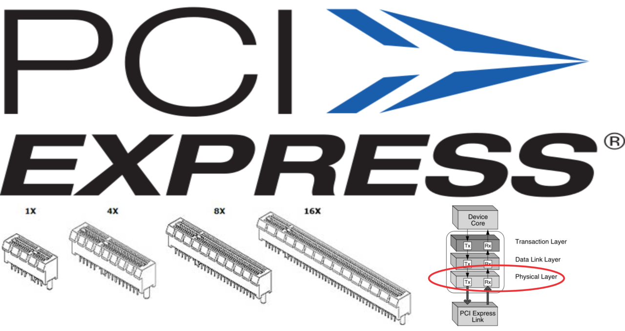
The lowest PCI Express architectural layer is the Physical Layer. This layer is responsible for actually sending and receiving all the data to be sent across the PCI Express link. The Physical Layer interacts with its Data Link Layer and the physical PCI Express link.
This layer contains all the circuitry for the interface operation: input and output buffers, parallel-to-serial and serial-to-parallel converters, PLL(s) and impedance matching circuitry. It also contains some logic functions needed for interface initialization and maintenance.
In the physical layer let’s subdivide in two sub-blocks: Logical and Electrical sub-block
Logical Sub-Block
The logical sub-block is the key decision maker for the Physical Layer. The logical sub-block has separate transmit and receive paths, referred to hereafter as the transmit unit and receive unit. Both units are capable of operating independently of one another.
The primary function of the transmit unit is to prepare data link packets received from the Data Link Layer for transmission. This process involves three primary stages: data scrambling, 8-bit/10-bit encoding, and packet framing. The receive unit functions similarly to the transmit unit, but in reverse. The receive unit takes the deserialized physical packet taken off the wire by the electrical sub-block, removes the framing, decodes it, and finally descrambles it.
The figure below illustrate this:

Remember that you need to consider each lane of the PCIe.
Some sub topics in the electrical sub-block:
- Data Scrambling – PCI Express employs a technique called data scrambling to reduce the possibility of electrical resonances on the link. PCI Express specification defines a scrambling/descrambling algorithm that is implemented using a linear feedback shift register. PCI Express accomplishes scrambling or descrambling by performing a serial XOR operation to the data with the seed output of a Linear Feedback Shift Register (LFSR) that is synchronized between PCI Express devices
- 8-Bit/10-Bit Encoding – The primary purpose of 8-bit/10-bit encoding is to embed a clock signal into the data stream. By embedding a clock into the data, this encoding scheme renders external clock signals unnecessary.
- Packet Framing – In order to let the receiving device know where one packet starts and ends, there are identifying 10-bit special symbols that are added and appended to a previously 8-bit/10-bit encoded data packet
Electrical Sub-Block
As the logical sub-block of the Physical Layer fulfils the role as the key decision maker, the electrical sub-block functions as the delivery mechanism for the physical architecture.
The electrical sub-block contains transmit and receive buffers that transform the data into electrical signals that can be transmitted across the link.
The electrical sub-block may also contain the PLL circuitry, which provides internal clocks for the device.
Some sub topics in the electrical sub-block:
- Serial/Parallel Conversion – The transmit buffer in the electrical sub-block takes the encoded/packetized data from the logical sub-block and converts it into serial format. Once the data has been serialized it is then routed to an associated lane for transmission across the link. On the receive side the receivers deserialize the data and feed it back to the logical sub-block for further processing.
- Clock Extraction – In addition to the parallel-to-serial conversion described above, the receive buffer in the electrical sub-block is responsible for recovering the link clock that has been embedded in the data.
- Lane-to-Lane De-Skew – The receive buffer in the electrical sub-block de-skews data from the various lanes of the link prior to assembling the serial data into a parallel data packet. This is necessary to compensate for the allowable 20 nanoseconds of lane-to-lane skew.
- Differential Signaling – PCI Express transmit and receive buffers are designed to convert the logical data symbols into a differential signal.
- Phase Locked Loop (PLL) Circuit – A clock derived from a PLL circuit may provide the internal clocking to the PCI Express device. Each PCI Express device is given a 100 mega-hertz differential pair clock. This clock can be fed into a PLL circuit, which multiplies it by 25 to achieve the 2.5 gigahertz
- AC Coupling – PCI Express uses AC coupling on the transmit side of the differential pair to eliminate the DC Common Mode element. That makes the buffer design process for PCI Express becomes much simpler
- De-Emphasis – PCI Express utilizes a concept referred to as de-emphasis to reduce the effects of inter-symbol interference.
As always, leave a comment if you want me to get into more details.
Share this post via:


TSMC CoWoS versus Intel EMIB Semiconductor Packaging