The most vexing problem for physical implementation engineers is debugging errors due to power-ground “shorts”, as reported by the layout-versus-schematic (LVS) physical verification flow. The number of polygons associated with each individual grid is large – an erroneous connection between grids results in a huge number of segments reported by LVS analysis. These connection issues can arise from a number of sources – e.g., an error in coding the P/G grid segments or signal track locations in the setup file for a block-level place-and-route step, a miscalculation in a via array generation script, or an incorrect metal fill algorithm.
Mentor, a Siemens Business, recently published an app note describing a straightforward methodology for detecting P/G shorts, utilizing a couple of routines released with their Calibre tools. The goal is to enable a quick turnaround method focused on P/G physical design issues. The intent is to exercise this flow often – e.g., running at block level after an iteration of place-and-route, or running at the full-chip SoC level with (potentially) partial block data. Although the error dataset for a P/G short can be large, fortunately, the errors tend to be systematic. The fixes to the P&R grids, routing tracks, and/or the insertion algorithms are typically relatively easy to re-code. By simplifying the task of P/G connectivity verification – “shifting left”, in common parlance – debugging the final LVS results with full-chip SoC data will be expedited.
Using Layer-Purpose Pairs to their Fullest
The Mentor flow utilizes the feature of GDS-II or OASIS physical data to represent each object with both its fabrication layer designation plus an additional attribute – a “purpose” (or datatype). Together, these are known as the (layer-purpose) pair for the object. The figures below illustrate the proposed flow.
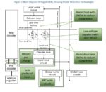
Figure 1. Overview of P/G connectivity checking flow
At a high level, the physical design data is exported from a block’s P&R results in LEF/DEF format, and mapped to specific layer-purpose pairs for subsequent LVS connectivity checks.
From the LEF/DEF data, it is necessary to identify the power and ground nets from the SPECIALNETS section of the DEF file, as shown in the figure below.
Figure 2. Example of the SPECIALNETS section in the DEF file from a P&R flow
The Mentor utility code then assigns the (layer, purpose) pair attribute to all data on each metal level, as shown below.
Figure 3. Mapping table for different classes of metal nets and pins, using layer-purpose pairs
Parenthetically, it is pretty common for complex custom layouts to use lots of additional layer definitions in the design composition palette – e.g., MnVDD, MnGND, MnVDDIO, MnGNDIO – each with different visual setting for color and stipple pattern. The layout designer utilizes these distinctions when drawing to try to avoid connection errors. The same Mentor approach applies here, as well, where the individual palette layers would be mapped to the (layer, purpose) pairs in the table above.
Once the exported physical design data is separated into (layer, purpose) subsets, the Mentor Calibre SVRF verification runset exercises the appropriate “shorting” and “bridging” connectivity checks, as depicted below.
Figure 4. Example of connectivity checks for P/G shorts and bridges
Additionally, there is an interactive Calibre debug feature which helps to quickly identify the cause of the connectivity error. A shape that is identified as part of the error can be “isolated” in Calibre – still present in the physical data model, but assigned a different electrical net identifier. An interactive LVS short check routine can be rerun to investigate how the connectivity error is affected.
The Mentor Calibre app note on LVS P/G shorts verification can be accessed at the following link. The interactive debug method for virtual isolation of a selected shape prior to re-running LVS is shown in this online video demonstration (link).
Also Read:
Mentor Offers Next Generation DFT with Streaming Scan Network