RVN! 26 Banner revised (800 x 100 px) (600 x 100 px)

Why Near-Threshold Voltage is an Excellent Choice for Hearables

Why Near-Threshold Voltage is an Excellent Choice for Hearables
by Lauri Koskinen on 05-05-2021 at 6:00 am

blog part 3 energy frugality graphic FINAL 1

In the previous blogs on this topic, we’ve seen that utilizing near-threshold voltage (NTV) saves incredible amounts of energy, theoretically up to 10x and in practice from 2x to 4x. But there is a price which makes some applications more suited for NTV than others. This is due to the inevitable performance (speed) loss of NTV as transistor current decreases with respect to operating voltage. While some applications require full speed all of the time, almost all IoT applications have widely varying performance requirements. Here, I’ll dig into one of the hottest IoT applications which happens to be an excellent fit for NTV: wireless audio hearables, also known as true wireless systems.

To be state-of-the-art in the very competitive hearables space, the system must include Keyword Spotting (KWS) such as Alexa or Siri. These are always-on systems: because the keyword can come at any random time, the system cannot be (completely) shut down. This already rules out long sleep times, the most common energy saving method of IoT systems. A typical KWS system consists of a feature extractor and a neural-network-based classifier, a form of artificial intelligence (AI). For energy efficiency, these are usually preceded by an energy/voice activity detector. This allows for the system to run the low-performance energy detection as the only always-on component and only wake up (via interrupt etc.) the main processor when energy resembling speech is detected. Of these, NTV is an excellent choice for the energy detector.

In a conventional energy-optimized system, the energy detector is often a hardwired block. Ultimately, time-to-market demands programmability as algorithms and architectures change, and anything hardwired severely limits this. One option would be a “big-little” type of system: a small CPU sharing memory and periphery with a bigger CPU such as an Arm M0 and an Arm M33, or two RISC-V cores. But even this solution has task-switching limitations on memory and switching time. If your software team gets to decide, all tasks will be run on the same core. Then there’s the extra silicon and verification costs that go into a multi-core solution.

Minima’s approach to a NTV system makes a single-core solution possible, one that can scale its energy together with its performance. As seen in Figure 1, using all of the energy curve (and not just a small sliver at the top) allows for optimizing energy no matter how much performance spread your application requires such as with keyword detection in hearables.

Figure 1: Minima’s approach to NTV operation enables a CPU to scale its energy (shown on the right) for simple parts of an algorithm as well as the more complex parts such as in hearables IoT applications.

Even better, Minima’s approach to NTV system maximizes the use cases of the CPU. Modern KWS algorithms are heavily optimized for small, embedded-class CPUs but today’s deep-submicron processes mean that often there is still room left at the top for you to design the system for more performance. So, when your algorithm and SW guys want more performance for a product with a bigger battery, you can reuse the system.  For example, adding a 0.9V operating point in Figure 1 might allow for the same chip to be used as a speaker driver feedback DSP. Greater task granularity in your application may also be possible; for example, running different Bluetooth layers or neural-network layers at different operating points.

These examples of being energy frugal apply to a large number of other applications. Anywhere you need AI, there are probably energy-saving possibilities by using simpler algorithms part of the time enabled by Minima’s approach to a NTV system.

https://minimaprocessor.com/


Transistor-Level Static Checking for Better Performance and Reliability

Transistor-Level Static Checking for Better Performance and Reliability
by Daniel Payne on 05-04-2021 at 10:00 am

power intent checks min

My first transistor-level IC design job was with Intel, doing DRAM designs by shrinking the layout to a smaller process node, and it also required running lots of SPICE runs with manually extracted parasitics to verify that everything was operating OK, meeting the access time specifications and power requirements across PVT corners. I’d do a SPICE run, and show the waveform and timing results to a senior circuit designer, and then he’d ask for the schematics and say, “Go and make this change, then rerun SPICE again.” What a slow and laborious process it was to migrate a high-volume memory part. Eventually I learned the art and science of DRAM design, and then became a senior circuit designer, responsible for eyeballing other designers schematics, reviewing their waveforms, and telling them, “Go and make this change, then rerun SPICE again.”

The EDA industry has paid attention to the challenges of transistor-level circuit designers over the years and has come up with something beyond just running lots of SPICE circuit simulations, and that tool category is known as static checking, which is something that complements what SPICE can tell you. A new white paper from Siemens EDA was just released on static checking, and I’ll give you an overview of what static checks can help you quickly verify.

Power-Intent Checks

IP blocks within an SoC can employ many power domains, and that requires some transistor-level design control with:

  • Voltage regulators
  • Header and footer switches
  • Level shifters
  • Isolation cells
  • State retention cells

In the following block diagram the circuit designer needs to place and verify that there is a level shifter between the power domains connected to VCC1 and VCC2, transistors with thick oxide are connected to the high voltage supply, and that an isolation cell is placed between Block 2 and 3, because Block 2 has gated power.

A static checker can automatically detect every power domain crossing in a chip, and verify that level shifters and isolation cells are properly placed. You really want to be using a transistor-level verification tool for tricky tasks like this to ensure thorough verification. Catching and fixing a power intent bug before tape out makes economic sense.

ESD Protection Verification

I remember placing DRAM chips onto a tester during characterization, and we always wore a conductive strap connected to the tester, which prevented the build up of Electro Static Discharge (ESD) while walking on the carpet, that created a large voltage that potentially damaged the IC as current flowed into the chip. IO cells on a chip using multiple power domains have special diodes to shunt the high ESD currents away from rest of the chip.

A static checker can find all of these ESD elements, including parasitic resistances and capacitances, and calculate ESD safety limits much faster than running an exhaustive number of SPICE simulations. Vias on interconnect layers in the ESD path can be statically checked for electromigration compliance.

Voltage-Aware Spacing Checks

There’s a reliability concern called Time-Dependent Dielectric Breakdown (TDDB), where the allowed spacing of wires is dependent of the voltages of the wires.

A typical DRC tool doesn’t know about voltages, and trying to run dynamic SPICE simulations on a full chip isn’t practical, so the smarter approach is using a tool that can do static voltage propagation and topology checks for TDDB.

Analog layout-dependent checks

AMS designers know about taking layout precautions to ensure robust operation, like:

  • Device layout symmetry
  • Current orientation matching
  • Dummy device insertions
  • Common centroid and pitch between devices
  • Electrical parameter matching

In the following schematic for a fully differential mixer the layout designer needs to use symmetry between:

  • M1, M2, M4, M5
  • M3, M6
  • M7, M8
  • RI

Small layout differences can impact performance, while a static checker can quickly identify any layout dependent violations.

Summary

Yes, SPICE circuit simulation is still heavily used for transistor-level IP design and verification, but using advanced, FinFET process nodes, there are so many more effects to verify now that it makes sense to add a static checker to ensure that your designs are meeting power intent, ESD protection, voltage-aware spacing, and analog layout-dependent effects. Using the right tool for the right task makes the life of a chip designer less stressful, and ensures that silicon will perform to spec, and operate reliably.

The full white paper is online here.

Related Blogs


Achronix Next-Gen FPGAs Now Shipping

Achronix Next-Gen FPGAs Now Shipping
by Kalar Rajendiran on 05-04-2021 at 6:00 am

1980s to Now Market Changes

Earlier in April, Achronix made a product announcement with the headline “Achronix Now Shipping Industry’s Highest Performance Speedster7t FPGA Devices.” The press release drew attention to the fact that the 7nm Speedster®7t AC7t1500 FPGAs have started shipping to customers ahead of schedule. In the complex product world of semiconductors, hitting a production silicon milestone ahead of schedule is a significant accomplishment. The copy stated that the product includes innovative architectural features making it ideal for data acceleration applications. It also spotlighted the industry’s first 2D network-on-chip (NoC), an architectural innovation that eliminates complex routing bottlenecks found in traditional FPGAs. Amid these highlighted aspects, it is easy to miss the bigger story.

No, I’m not talking about the upcoming SPAC merger with ACEV to become a publicly traded company. Yes, that’s a significant story as well and portends to bring lot of benefits to Achronix’s customers. But there is an even bigger story. And that story is about the effect Achronix’s solutions and product strategy are expected to have on the industry. In order to fully appreciate the potential impact, we have to review the changes that have taken place from the 1980s to today. That backdrop will provide the rationalization for what, why and how Achronix’s timeless solutions are expected to solve long standing chronic problems.

1980s to Now

Market Evolution:

There was a time when integrated circuit (IC) chips used to be referred to as computer chips. That is because there was only one market and that was the computing market. Product performance was critical. Cost and power consumption were secondary. That was the situation, say up through the 1980s. From the 1990s, communications market started growing rapidly. Product performance was still a dominant driver although cost also started becoming important. From the 2000s, consumer market for electronic products started growing rapidly. Cost and power consumption became dominating factors. The late 2000s saw the lines between computing, communications and consumer markets fade away in a major way. From the 2010s, big data, e-commerce, data security and cloud computing became major drivers. And starting around 2015, we entered the artificial intelligence (AI) era and emphasis of edge computing paradigm. Refer to Figure below.

But this evolution did not lead to a super-monolithic market segment. On the contrary, a number of smaller market segments have been created with requirements primarily driven by the use case the devices are deployed for.

Semiconductor process node/technology:

In order to support the above market evolution, foundries have been pushed to develop multiple flavors of a process node, one for high performance/speed, one for low power, one for ultra-low power, etc.,

Chip Design Cost and Cycle Times:

With the introduction of each advanced process node, chip design cycle time got longer. And chip design cost went higher.

Market Attraction for ASICs:

ASIC-based product attractiveness was a no brainer when the target market segment was large, the development cost was low and the design cycle time was short. This was the case up until the early 2010s. As the market evolved, monolithic large market segments fragmented into many smaller ones. This combined with increased development cost and longer design cycle time, made it difficult to make a business case for ASICs.

Product Cycles:

Electronic product cycles that used to be around three years back in the 1990s started getting shorter and shorter. With explosive growth in AI driven applications and rapid advances in AI techniques, product cycles got compressed tremendously.

Market Attractiveness for traditional FPGAs:

Although the founding of the ASIC market and the traditional FPGA market happened in the 1980s, both markets did not experience the same growth path. For a long period, FPGAs were predominantly used for prototyping and in low-volume, high-margin products. It remained this way until the communications market started taking off and high-speed I/O were added to FPGAs.

Chronic Problems:

Processors: Consume too much power as a tradeoff for maximum flexibility

ASICs:           Lack of flexibility (once implemented) as a tradeoff for optimized performance and power

Traditional FPGAs: Not as optimized as ASICs, not as flexible as processors, intrachip performance bottlenecks.

ASSPs:          Not as optimized as ASICs as a tradeoff for amortizing R&D cost over a larger market

Now and Onward

What if we can solve the chronic problems without too much of a tradeoff? How about increasing addressable market size and extending product life without having to re-spin silicon?

With the market moving toward an AI driven, edge-centric, fast-changing, data-accelerated product space with short life cycles, the stage is set for a timeless solution to fill the demand. The increased interest in leveraging a chiplet methodology for developing semiconductor products is not a coincidence.

Achronic (timeless) Solutions:

Achronix through its ACE design tools and partner tools ecosystem, makes it easy for customers to design their products. Customers may tap from the Speedster® family of products that eliminates traditional FPGA problems. Customers could also tap from Achronix’s various eFPGA cores to implement their products and eliminate other chronic problems. I expect product developers to adopt chiplets methodology and eFPGAs incorporation as and when applicable. In essence, customers could achieve earlier tape-out, address more SKUs and extend product lifecycle.

If you are developing products in any of these high-growth, fast changing markets (refer to above figure), you may want to explore ways to benefit from Achronix’s offerings by holding deep dive discussions with them.


You know you have a problem when 60 Minutes covers it!

You know you have a problem when 60 Minutes covers it!
by Robert Maire on 05-03-2021 at 2:00 pm

60 Minutes Chip Shortage

-Chip shortage on 60 Minutes- Average Joe now aware of chip issue
-Intel sprinkling fairy dust (money) on New Mexico & Israel
-Give up on buy backs and dividends
-Could Uncle Sam give a handout to Intel?

You normally don’t want to answer the door if 60 Minutes TV crew is outside as it likely doesn’t mean good things. But in the case of the chip industry, the shortage that has been talked about in all media outlets has finally come home to prime time.

The chip shortage that has impacted industries across the board from autos to appliances to cigarettes so it has gotten prime time attention;

CBS 60 Minutes program on Chip Shortage

60 Minutes got hold of some of our past articles including our recent ones about the shortage and China risks and contacted us.

We gave them a lot of background information and answered questions about the industry and shortages as we wanted to help provide an accurate picture.

Overall, we think they did a great job representing what was going on in the industry and were both accurate and informing.

Does Intel have its hand out?

We have previously mentioned that we thought that Intel was looking for government help and maybe a handout which was touched upon in Pat Gelsinger’s interview , up front. While certainly not directly asking for money, it certainly sounds like Intel wouldn’t say no. Intel was clearly shopping the idea under the previous administration in the White House as well as previous Intel management.

The chip shortage both amplifies that prior request as well as makes it more timely. It also gets even more timely when it is put under the banner of infrastructure repair.

Intel is going to hemorrhage Money

We have said that Intel’s financial’s were going to get a lot worse before they got any better.

We suggested they would triple spend 1) Spend to have TSMC make product 2) Spend to catch up to TSMC (like on EUV and other tools) 3) spend to build extra capacity to become a foundry.

Intel, Gelsinger, even said on 60 minutes that they are not going to be doing stock buy backs.

Intel in Israel & New Mexico

Intel has just announced that in addition the the $20B for two new foundries that it is spending in Arizona, it is spending $3.5B in New Mexico on packaging technology & capacity.

Intel is also spending $200M on a campus in Haifa, $400M for Mobileye in Israel and $10B to expand its 10NM fab in Kiryat Gat, Israel . Its interesting to note that the spend in Israel is not mentioned on Intel’s newsroom website as it likely doesn’t fit the “move technology & jobs back to the US” that Gelsinger espoused on 60 Minutes.

Between spending on production at TSMC, fixing Intel, building foundries, New Mexico, Mobileye, Israel (likely Ireland as well)…Intel is going to be raining down money all over.

Mark Liu on 60 minutes

Mark Liu was also interviewed as the clear leader in technology and capacity in the chip industry. We think that Liu was very accurate and straight forward when he said that TSMC was surprised that Intel had fumbled.

He also clearly is on the side of the industry that downplays the shortages and thinks they will be short lived.

As to the “repatriation” of the chip industry to the US, as expected he sees no reason for it.

He also stayed away from commentary about the “Silicon Shield” provided to Taiwan by its leadership in chips.

TSMC is clearly in the drivers seat and is not likely to change any time soon

The Stocks

Given the spending and gargantuan task ahead we have suggesting avoiding Intel’s stock as its going to both take longer and cost more than anyone suggests and the odds of success aren’t great.

Gelsinger is on a world tour sprinkling fairy dust around which he will need the luck of as we go forward.

We would not be surprised if the government does indeed write Intel a check as they are the US’s only and last hope of getting back in the semiconductor game which is so critical to our future, not to mention our short term needs.

All this spend will do zero to help the shortage but the shortage did at least bring these issues (many of which we have been talking about for years) to the forefront of peoples minds.

We do continue to think that the semi equipment industry will likely benefit big time especially ASML as they have a lock on EUV.

We also think equipment companies can make a few bucks on their old 6″ and 8″ tools if they can resurrect manufacturing as those are the fabs in shortest supply.

Also Read:

KLAC- Great QTR & Guide- Foundry/logic focus driver- Confirms $75B capex in 2021

Lam Research performing like a Lion – Chip equip on steroids

ASML early signs of an order Tsunami – Managing the ramp


Synopsys Debuts Major New Analog Simulation Capabilities

Synopsys Debuts Major New Analog Simulation Capabilities
by Tom Simon on 05-03-2021 at 10:00 am

Synopsys analog simulation

Just prior to this year’s Synopsys User Group (SNUG) meeting, I had a call with Hany Elhak, Group Director of Product Management and Marketing at Synopsys, to talk about their latest announcements for analog simulation. Synopsys usually has big things to talk about each year around this time – this year is no exception. Hany had a set of announcements to discuss that represent a major leap forward for their entire analog simulation lineup.

Under the moniker of PrimeSim Continuum they are rolling out a unified workflow for all their circuit simulation technologies, a GPU accelerated SPICE and a new FastSPICE architecture. Hany talked about how over the last 5 years advanced node SoCs have changed so that increased capacity and speed is needed for transistor level simulation. IOs are running at data rates over 100 Gb/s, embedded memories are larger and faster, and analog/custom content is increasing steadily. All of these factors and others are translating into the need to perform more analog simulations across many parts of today’s SoCs and their memory subsystems.

Synopsys analog simulation

Previously there has been a balkanization of analog simulation technologies for each domain, such as libraries, memories, power distribution networks, IO circuits, etc. Likewise, with the rate of CPU performance-scaling slowing down the increases in capacity and throughput needed to keep up with design size and multi-corner analysis have not been available. Advanced process node designs have experienced reduced margins and increased parasitics, making analog simulation analysis even more important.

For the first time ever, Synopsys is taking advantage of GPUs to gain massive performance improvements. GPUs always seemed like they could offer big performance gains, but until they supported high precision floating point they were not suitable for SPICE. GPU performance year-to-year is moving at factor of 1.5, which means that by 2015 they will offer a 1000X performance advantage over CPUs alone. Of course, Synopsys has improved the overall performance of PrimeSPICE by 3X in the newest release, and there is good scaling with additional CPUs. However, adding GPUs can add an additional 10X over this.

PrimeSim Pro, their FastSPICE offering, now has a new architecture that runs 2-5X faster and can scale to handle billions of elements, opening the doors to running on larger designs for more complete SoC and memory subsystem verification. GPU acceleration is also available now in PrimeSim Pro. Synopsys has enhanced power block detection, optimized event propagation, and developed core independent partitioning for PrimeSim Pro. There are also improvements in advanced modeling. It supports math-based load models, net based coupling cap handling, and has a new RC reduction algorithm. These changes open up capacity for massive PDNs and simulation with full parasitics. In particular Hany pointed out how this will enable full simulation of multi-die SoC memory subsystems. His example showed full simulation of six 16 Gb die and their controller.

All of this would still be cumbersome to set up, run and interpret results without a unified simulation environment. Synopsys also announced PrimeWave, which provides a comprehensive environment for all advanced analyses. It works with all the PrimeSim Continuum simulators for all modes of analysis. According to Hany, it will be used for analog, memory, signal/power integrity and RF. PrimeWave has integrated waveform viewing and post processing, inside a flexible and programmable environment.

PrimeSim Continuum is tightly coupled with Custom Compiler for analog design acceleration. It is also integrated with VCS so mixed simulation will be easier and faster. Lastly, IP characterization will also benefit from PrimeLib’s integration into this design platform.

As is always the case, Synopsys has done extensive work during their product development with leading semiconductor companies to ensure the flow is fully tested and meets end user requirements. Their announcement is accompanied with endorsements from KIOXIA, Samsung Memory, NVIDIA and Samsung Foundry. They each report consistent improvements in runtime and accuracy. They also point to the common workflow as a big step forward in productivity.

Synopsys continues to maintain its track record for innovation and investment in its leading suite of circuit simulation tools. This should come as no surprise to anyone, but the ambitious changes in this announcement are gratifying to see. What is especially interesting is that they are making use of the formidable power of GPUs for the first time. GPUs offer massively parallel computing for applications that can be architected to take advantage of them. With GPUs now supporting double precision floating point operations and high capacity and bandwidth memory, they are now an excellent vehicle for SPICE based simulation.

The full announcement and all the details are available on the Synopsys website.

Also Read:

Accelerating Cache Coherence Verification

Addressing SoC Test Implementation Time and Costs

Your Car Is a Smartphone on Wheels—and It Needs Smartphone Security


Intel’s EMIB Packaging Technology – A Deep Dive

Intel’s EMIB Packaging Technology – A Deep Dive
by Tom Dillinger on 05-03-2021 at 6:00 am

EMIB configurations

The evolution of low-cost heterogeneous multi-chip packaging (MCP) has led to significant system-level product innovations.  Three classes of MCP offerings have emerged:

  • wafer-level fan-out redistribution, using reconstituted wafer substrates of molding compound as the surface for interconnections between die (2D)
  • a separate silicon-based interconnect layer for redistribution, either a full-sized silicon interposer or die-to-die silicon bridges embedded in the organic package (2.5D)
  • face-to-face or face-to-back die stacked vertically, utilizing hybrid bonding of die pads, with through-die vias (3D)

The 2.5D solution has received considerable R&D investment, to support larger package sizes and greater interconnect redistribution density (i.e., line + space pitch, number of metal layers).  The integration of multiple, smaller die provides chip and package assembly yield and cost tradeoffs.

The functionality integrated in the 2.5D MCP has become increasingly diverse – e.g., CPUs, GPUs, memory (especially HBM stacks), FPGAs, network switches, I/O transceivers, hardware accelerators for specific applications.  Current R&D efforts will continue to extend the breadth of this system-in-package composition – the next “big thing” could likely be the integration of optoelectronic conversion elements, enabling the efficiencies of photonic-based data transfer over medium- and short-range lanes.

A key facet to enabling the growth of 2.5D MCP offerings is the technology for the internal connectivity between die in the package.  As mentioned above, one alternative is to fabricate the wires on a silicon interposer, whose dimensions equate to the full package size.  Recent advances have enabled interposers to exceed the 1X maximum reticle size for die placement and interconnect.  Another is to fabricate a small silicon bridge for the wires, embedded in an organic package, spanning the edges of adjacent die.

Intel’s Embedded Multi-Die Interconnect Bridge (EMIB) is an example of 2.5D MCP bridge interconnect technology.  It has been briefly described in previous SemiWiki articles (link).

With the recent re-introduction of Intel Foundry Services, I thought it would be appropriate to dive a bit more deeply into this technology, as it will no doubt be a fundamental part of ICF customer system implementations.

I had the opportunity to learn more about EMIB capabilities and potentials, in a most enlightening discussion with Ravi Mahajan, Intel Fellow in Assembly and Test Technology Development.  This article summarizes the highlights of our discussion.

EMIB Fabrication

The figure above illustrates a cross-section of a typical EMIB bridge resident in the organic package.  The bridge silicon resides in a package cavity, fabricated as depicted in the figure below. The top package metal layer provides a reference plane, with vias through the plane connecting the die and bridge.


Ravi indicated, “The EMIB process is built upon the standard package construction flow, with the additional steps to create the EMIB cavities.  The bridges are positioned in the cavities, held in place with an adhesive.  The final dielectric and metal build-up layers are added followed by via drilling and plating.”

Note in the cross-section picture above the reference to coarse and fine vias, corresponding to the two different bump pitches present on each die, as shown below.

The coarse bumps are used for die-to-package trace layer connections, while the fine pitch is associated with the EMIB connections – more on the target EMIB connection density shortly.

Ravi added, “Considerable engineering effort was invested to define the fine and coarse bump profiles that would support die attach and via connection processing.  Specifically, that included focusing on bump height control and solder volume.  We have worked with bumping providers to enable this dual pitch and profile configuration.  In addition, each die in the MCP package is attached individually – the bumps on the die will be subjected to multiple reflow cycles.  Attention was paid to the flux materials incorporated with the bumps.  A process to provide void-free epoxy underfill throughout the bump regions has also been developed.  The materials, bumps, and the attach process are all in high volume manufacturing.”

EMIB Physical Implementation

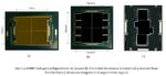
An example of a fabricated bridge is shown below.  This specific design implements the following:

  • 55um bump pitch to the die above
  • 2um line + 2um space, with 2um metal thickness
  • 4um pitch, with 250 wires per mm “beachfront”
  • 2um thick dielectric between each EMIB metal layer
  • 4 metal layers on the EMIB bridge, M1 and M3 are dedicated to GND planes
  • signal layers that typically utilize a 3 signal + 1 ground shield pattern on M2 and M4

To be precise, the metal planes on the alternate EMIB layers are implemented as a mesh, as depicted below.

Ravi said, “The design of the EMIB interconnects is an intricate tradeoff between multiple targets – the interconnect density (wires per die edge per mm, bumps per mm**2), power constraints, and signaling bandwidth.  For each die, that implies driver sizing and receiver sensitivity.  For power savings, an unterminated receiver is typically used (i.e., capacitive load only, no resistive termination).  To address those targets, the EMIB design considerations include line and space dimensions, bump pitch, channel length, metal thickness, and dielectric material between the metal layers.  The design of the electrical signal shielding (e.g., S1G1, S2G1, S3G1) is also crucial.”

The figure below shows the layout view of the interconnect density design, including how the bridge signals reach multiple rows of fine-pitch bumps on adjacent die.  The table below illustrates the range of dimensions and pitches available.

The figures below show various bridge positioning options.  Note that there is considerable flexibility in bridge placement – e.g., horizontal and vertical orientations, asymmetric locations relative to die edges.

EMIB Electrical Characteristics

Intel has published a detailed electrical analysis for the EMIB interconnect, evaluating insertion loss and crosstalk for various signal-ground shielding combinations and wire lengths. (References appended at the end of this article.)

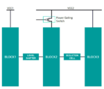
The figure above highlights the power distribution paths in the package.  Note that the small footprint of the EMIB bridge means the balance of the I/O signal and power integrity characteristics are unaffected, unlike a full silicon interposer where all signal and power vias must first traverse through the interposer.  As mentioned earlier, the top package layer above the EMIB serves as a ground plane, as well.

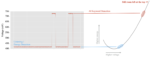
The figure below shows an example of the electrical analysis results, depicting the maximum EMIB signal length for a target cumulative beachfront bandwidth for various signal shielding patterns.  Aggressive L/S wire pitch designs were assumed for this example.  The electrical model used:

  • a simple output driver (R=50ohms, C=0.5pF)
  • an unterminated receiver (C=0.5pF)
  • four-layer EMIB metal stack-up, dielectric constant=4.0
  • top package metal plane above the embedded bridge
  • a 1V signal swing with a 200mV vertical eye opening receiver sensitivity (incorporating the near-end and far-end crosstalk for the unterminated, capacitive receiver)

EMIB Design Services

Due to the intricacies of the EMIB design tradeoffs, Ravi indicated, “Intel will collaborate closely with the foundry customers on their product requirement, and develop the EMIB designs as a service.  We will work with the customers on die pinout and bump patterns, and provide the EMIB silicon implementations that address their datarate targets.” 

EMIB Future Development

EMIB technology continues to be an R&D focus at Intel.  Ravi highlighted, “We will continue to work on providing greater interconnect edge density, including tighter bump pitch and more aggressive line/space EMIB metal pitch (sub-1um).  It’s certainly feasible to incorporate active circuitry into the EMIB, as well.”

Summary

The EMIB bridge approach in support of advanced MCP technology offers some unique advantages:

  • extension of existing organic packaging technology
  • enables large die count and large package configurations
  • lower cost than a full-size silicon interposer
  • support for high datarate signaling between adjacent die, using simple driver/receiver circuitry
  • ability to optimize each die-die link individually by customizing the bridge for that link

The EMIB links are power-efficient, with low metal R*C delays, with minimal latency and high signal integrity.

There are some EMIB disadvantages, which have been addressed by the Intel R&D team:

  • additional complexity in the die bumping and package assembly process
  • disparate coefficient-of-thermal-expansion (CTE) factors between the package, the die, and the EMIB bridge

The EMIB silicon is thinned prior to package assembly (t < 75um), and thus doesn’t significantly alter the thermally-induced mechanical strain between package and die and the bumps plus underfill interface.  The overall reliability is comparable to a conventional organic package.

The support provided by the packaging team at the Intel Foundry Services will assist customers seeking advanced MCP solutions to achieve their signaling datarate, power, and cost targets.

The growth of MCP packaging adoption will no doubt continue to accelerate.  (The DARPA CHIPS program will also contribute to greater interest in MCP design.)

For more information on Intel’s EMIB offerings, please follow this link, and be sure to consult the references below.

-chipguy


References

[1] Mahajan, R., et al., “Embedded Multi-Die Interconnect Bridge (EMIB) – A High Density High Bandwidth Packaging Interconnect”, 2016 IEEE 66th ECTC conference, p. 557-565.

[2]  Durgun, A., et al., “Electrical Performance Limits of Fine Pitch Interconnects for Heterogeneous Integration”, 2019 IEEE 69th ECTC conference, p. 667-673.

[3]  Mahajan, R., et al., “Embedded Multidie Interconnect Bridge – A Localized, High-Density Multichip Packaging Interconnect”, IEEE Transactions on Components, Packaging, and Manufacturing Technology, Vol. 9, No. 10, October, 2019, p. 1952-1962.


KLAC- Great QTR & Guide- Foundry/logic focus driver- Confirms $75B capex in 2021

KLAC- Great QTR & Guide- Foundry/logic focus driver- Confirms $75B capex in 2021
by Robert Maire on 05-02-2021 at 10:00 am

KLAC Foundry Logic

– KLA put up an excellent quarter and Guide
– Rising above the increasing tide of orders
– Confirms $75B capex in 2021 with upside
– Foundry & Logic continue to be the sweet spot for KLA

Business is very very good and getting better

-Revenues came in at $1.8B with EPS of $3.85, all above the range
-Guidance is for $1.855B+-$100M with EPS of $4.08/ These are superb numbers any way you look at it.
– Gross margin was at 62.9% and operating margin of 40.4%
– $585M or 97.8% free cash flow conversion

KLA remains a stand out leader in process control with 53% market share

Both wafer inspection and patterning were up over a third from last year. Surprisingly Korea was 31% versus Taiwan’s 22%. The only light area was process equipment which was up only 12% Y/Y, which trailed the market as compared to KLA’s core business.

Benefit from EUV rollout continues

KLA continues to see increased business as EUV rolls out at different customers. KLA’s 5th generation tools are adopted to help with the increasing roll out.

In our view, the good order news coming out of ASML for tools translates a little bit later to more process control tools for KLA. In our view KLA always tends to follow in the footsteps of ASML’s order pattern and it looks very strong.

$75B in WFE capex for 2021?

KLA management suggested that WFE spend in 2020 was about $61B and that 2021 would be up in the low to mid twenties we we take to mean about $75B. This is more or less in line with what we and the rest of the industry are initially thinking. We could see that number finish up higher but right now its a good number to use.

KLA benefits from strong Foundry/Logic

As we have said many times before, KLA is the poster child for foundry/logic spend and that is what we are seeing right now. While memory remains OK, foundry/logic is out performing and will continue to outperform given the perceived shortage and secular growth drivers.

Memory may come back in the latter part of the year, maybe…, but for now it remains in the sweet spot of KLA’s business model

Financial performance remains top in the sector

As compared to the rest of the semiconductor equipment group KLA remains the top performer on all financial metrics. Aside from the fundamental growth in the stock price, everything is as good as it gets. KLA retains its ATM machine like cash behavior which is reflected in the stock price.

The Stock
The stock traded down slightly in the after market despite the fantastic report.
As we had projected earlier, there was a high degree of pressure and burden on KLA to put in performance that was well above and beyond expectation.
The problem is that expectation has been growing by leaps and bounds and grew to an unreachable point in our view. It was all but impossible to get to a number that would make the street happy.

In general, we think the group as a whole is at a point where the valuations have to take a rest and catch up with themselves. Valuations are priced well beyond perfection so perfect performance isn’t good enough.

We might look for entry points to get in the stock if we had some weakness or other non company specific down drafts.

Also Read:

Lam Research performing like a Lion – Chip equip on steroids

ASML early signs of an order Tsunami – Managing the ramp

It’s not a Semiconductor Shortage It’s Demand Delirium & Poor Planning


Ireland – A Model for the US on Technology

Ireland – A Model for the US on Technology
by Scotten Jones on 05-02-2021 at 6:00 am

Slide1 2

After I published a recent article about Intel, I was contacted by the Irish Development Agency (IDA) where Intel has a large fab presence and asked if I would like to interview them about the Intel site. The interview with Turlough McCormack of the IDA, started with Intel’s presence in Ireland but then went on to paint an interesting picture of a country successfully attracting high technology companies. I thought this is interesting not only for what it offers high tech companies but also as a model for the US.

Intel in Ireland

Intel has had a presence in Ireland for 32 years. Intel has 360 acres of land in Leixlip, a town near Dublin and from 1989 to 2015 Intel spent 8 billion euros on the site and between 2019 and 2021 is investing an additional 7 billion euros for a total investment of $15 billion euros. The site currently employs around 5,000 people and will reach around 6,600 people with the new investment. The latest investment will double Intel’s manufacturing space in Ireland, be a centerpiece of Intel’s 7nm manufacturing and be the most advanced fab in Europe.

Figure 1 summarizes the Intel Ireland site.

Figure 1. Intel Ireland

Ireland’s High-Tech Model

After discussing Intel’s presence, we went on to discuss what makes Ireland attractive for high-tech in general and wafer fabs in particular.

There is a lot of discussion going on in the US and Europe about our reliance on Asia in general and Taiwan in particular, for advanced semiconductors. Taiwan is in the middle of a drought and has been dealing with limited water availability for years not to mention being located on an earthquake fault line and the political uncertainty of their relationship with mainland China. Turlough pointed out it rains a lot in Ireland and there is no shortage of water, they also have plenty of power and broadband availability. Ireland is not on a fault line, has no natural disasters and a mild climate. I am also fairly sure England has no plans to invade Ireland unlike mainland China who regularly threatens Taiwan.

The Government of Ireland has a pro-business attitude and has for many years. As a small country companies have access to key decision makers. Ireland has one of the lowest corporate tax rates in the world at 12.5%.

Ireland has an open border policy and is actively trying to attract technical talent to the country with fast-track work permit programs.

The government, universities and science centers are all working together on research initiates and developing talent. The Science Foundation Ireland is funding research in semiconductors and photonics at the university of Cork.

With Brexit, Ireland is the only English-speaking country in the European Union and provides a gateway to Europe.

Figure 2 summarizes Irelands pro high-tech environment.

Figure 2. Ireland High-Tech Model.

There are approximately 70 semiconductor companies with a presence in Ireland accounting for over 9,000 jobs and over 14 billion euro a year in 2018 revenue. The 70 semiconductor companies include around 24 smaller Irish companies and 300 million euro of R&D.

Just in the last 12 months announcements have been made for:

  • Microchip R&D center in Cork providing 200 jobs.
  • Qualcomm 78 million euro R&D and chip design center.
  • Huawei 80 million euro investment that will result in 110 jobs

In the last few years Cadence, Maxim Integrated and Logitech have invested in Ireland. I also brought up Analog Device presence in Ireland is I believe their largest manufacturing site. He noted ADI has been in Ireland for 40 year and has employs around 1,000 people in Limerick.

Interestingly, although the US invests more capital into Ireland than Irish companies do into the US, Irish companies employ more people in the US than US companies do in Ireland. He pointed out that Ireland is enabling US companies’ expansion into Europe, not taking US jobs.

Conclusion

In conclusion, Ireland has positioned their country as a business friendly, English speaking gateway to Europe. I believe that a lot of their business friendly policies would be useful additions to US policy to in our drive to increase US based leading edge semiconductor manufacturing.

Also Read:

How to Spend $100 Billion Dollars in Three Years

SPIE 2021 – Applied Materials – DRAM Scaling

Kioxia and Western Digital and the current Kioxia IPO/Sale rumors


Podcast EP18: The Story Behind Combining Methodics and Perforce

Podcast EP18: The Story Behind Combining Methodics and Perforce
by Daniel Nenni on 04-30-2021 at 10:00 am

Dan and Mike are joined by Simon Butler, founder of Methodics and Brad Hart, CTO of Perforce. We explore the acquisition of Methodics by Perforce, including motivation, strategy and a look to the future. We also discuss some of the history of Methodics and how they became successful.

For further discussion, visit their blog The Future of Semiconductor Design.

Simon Butler General Manager, Methodics Business Unit
Simon Butler was founder and CEO of Methodics Inc, acquired by Perforce in 2020, and is currently the General Manager of the Methodics Business unit at Perforce. Methodics created IPLM as a new business segment in the enterprise software space to service the needs of IP and component-based design. Simon has 30 years of IC design and EDA tool development and specializes in product strategy and design.

Brad Hart Chief Technical Officer
As the CTO of version control, Brad is responsible for the product strategy of the Perforce version control product suite – including Helix Core, Helix4Git, Swarm, and other clients and plugins. Brad has more than 20 years of experience in high-tech companies focused on optimizing development pipelines. He specializes in software engineering process, design, and implementation.

The views, thoughts, and opinions expressed in these podcasts belong solely to the speaker, and not to the speaker’s employer, organization, committee or any other group or individual.


CEO Interview: Rich Weber of Semifore, Inc.

CEO Interview: Rich Weber of Semifore, Inc.
by Daniel Nenni on 04-30-2021 at 6:00 am

Rich Weber

Rich Weber co-founded Semifore in 2006 with Jamsheed Agahi. Rich has a long history of complex chip and system design at companies including Data General, Stardent, Silicon Graphics, StratumOne and Cisco Systems. He received an MS in Electrical Engineering and a BS in Computer Engineering from the University of Illinois, Urbana-Champaign. Rich’s pioneering work at Cisco formed the basis of what became the SPIRIT / Accellera SystemRDL1.0 standard in 2009. Rich is a long-standing member of the Accellera IEEE 1685 IP-XACT steering committee. He has a deep understanding of industry standards, including their limitations.

What drove you to form Semifore in 2006?
I’ve been responsible for system architecture throughout my career – things like how the hardware interacts with the operating system and embedded software. In virtually every project, I was the system architect responsible for defining the address map and how device drivers would interact with it across many different operating systems. My experience with all those projects led me to conclude that the hardware/software interface, let’s call it the HSI, was a source of significant risk in the development process.

I can recall working at Silicon Graphics on high-end graphics processors and supercomputers. Often, there would be a fire drill in our Monday morning meeting because someone changed a bit in one of the registers and all the regressions failed over the weekend. At that point, the documentation was out of synch with the design RTL and many header files were likely incorrect. Those changes were made with good intentions, but the result was always the same – chaos.

After that, I began working on high-performance networking designs at a startup. These designs had a much more complex HSI, probably a factor of ten times more complex than what I had seen at Silicon Graphics. Based on that, we decided to automate HSI generation – the RTL, design descriptions, verification files, device driver development and support for bench measurements.  The HSI represented a large portion of the design, so this automation had far-reaching impact on the overall project. In those days, there was no commercially available tool to perform this automation, so roughly half the effort of the design team was dedicated to building the necessary scripts.

This company was quite successful and ultimately bought by Cisco. Now, as part of Cisco, the networking designs we were working on became much larger. In those days, Cisco had a specific focus on engineering best practices to reduce re-spins and time-to-market for its complex ASICs. Since Cisco was the result of many acquisitions, there was a need to converge the design methodology at an enterprise level. As part of that effort, I championed the need for an automated system to guide the implementation of the HSI. This part of the design had clearly become much too large and complex to be done either manually or with ad-hoc scripts and spreadsheets.

A project to address this automation was created. While the work had a positive impact on the design projects at Cisco, I saw an opportunity to do so much more. Handling complex designs with large register counts is virtually impossible without sophisticated automation. I knew I could build such a system that would scale efficiently for the largest designs. Without such a system it is very likely there would be missed deadlines, late tape-outs and hidden bugs in the field. In fact, studies have shown that one out of seven chips are re-spun due to a problem with the HSI. So, I left Cisco and formed Semifore.

Tell us about Semifore, what is the impact of their products on chip design?
Advanced semiconductor designs have many components, including multi-core architectures, programmable peripherals and purpose-built accelerators. These design elements require a pathway for embedded software to communicate with them. This is the HSI and it forms the foundation for the entire design project. Building an HSI that is correct and reliable puts demands on many parts of the design team. Beyond building an accurate, robust register map, the validation of the interface needs to be complete, and all supporting information also needs to be complete since the software team will build device drivers and high-level firmware from these specifications.

The stakes are quite high regarding getting all these pieces done correctly. Unlike timing or power closure, which can be verified rigorously, the verification of the HSI is a multi-dimensional problem that is bounded only by the imagination of the software team. I have seen cases where, years after a chip was put into production, it became impossible to add a new feature.  Why? During the software update process, it was discovered a device driver couldn’t be written. This was because a subtle error in the address map didn’t allow for the functionality. This is something of a nightmare scenario since the only fix is to deploy a new version of the chip to all systems in the field needing the new feature.

Subtle errors can escape into production. The only viable way to minimize this risk is to build an HSI with robust automation to ensure a correct-by-construction result. Add to that automated and accurate dissemination of the information needed by all members of the design team and you have a winning methodology. This is the methodology delivered by Semifore.

Scalability is another real problem for this kind of methodology. A typical HSI may contain millions of registers. The design team will require updates to these registers often, many times a day for example. The process of generating all this information needs to be extremely efficient, or the whole system will collapse under its own weight. The Semifore methodology can generate a five million register HSI in a matter of minutes. Problem solved.

This is the mission of Semifore. Deliver a winning methodology to allow design teams to focus on innovation, knowing the HSI is complete, robust and well-understood by everyone. The result is significantly lower risk, improved time-to-market and superior performance. In fact, without a methodology like this the chances of a working design are quite low.

A final question – How does Semifore fit with existing standards?
Standards provide great benefit. We fully support these efforts at Semifore, and I’ve personally been involved in the development of many standards. But standards cannot realize the ultimate goal, which is to develop an executable specification of the design. An executable specification is the only way to capture design intent and ensure a correct-by-construction HSI. Design teams maintain specifications in formats such as SystemRDL, IP-XACT and large spreadsheets.

These are all useful, but individually and even together they are missing many of the constructs needed to create a true executable specification and this is why standards fall short. Let me give you some examples. Moving up the level of abstraction and letting tools do the heavy lifting delivers a great productivity boost. To do this, programming constructs such as IF statements, LOOPS and CASE statements are needed, but they aren’t supported by existing standards. Often, the design may require a certain structure be imposed on a set of registers and the structure be captured in memory instead of flip flops. This is what is referred to as virtual registers. This is also not supported by existing standards.

To address these requirements, Semifore developed a domain-specific language called CSRSpec™. This language supports all the constructs mentioned and many, many more. It evolves with design requirements in real time, whereas a standard language would take years to encapsulate new requirements. CSRSpec includes over 200 unique properties and 6,000 register behavior combinations and complements existing standards and adds many more needed capabilities, so design intent can be accurately captured to create that all-important executable specification.

The CSRCompiler™ system generates high quality synthesizable RTL and all the support files needed to build the complete HSI and associated software drivers. CSRCompiler supports customization with a robust output tailoring capability that doesn’t require scripting. Through many years of development, CSRCompiler delivers extensive error checking and validation, with over 1,000 checks built in. All inputs are verified for semantic and syntactic correctness. Design practices that can lead to sub-optimal results are also flagged. This entire system can scale effortlessly to handle the largest, most complex designs.

This is the winning methodology I referred to. It provides the margin of victory for Semifore’s many customers across a diverse set of disciplines. We support many promising startups and large enterprises such as Microsoft as well. I am very proud of our accomplishments and our growing customer base.

Also Read:

CEO Interview: Dr. Rick Shen of eMemory

CEO Interview: Kush Gulati of Omni Design Technologies

Executive Interview: Casper van Oosten of Intermolecular, Inc.