
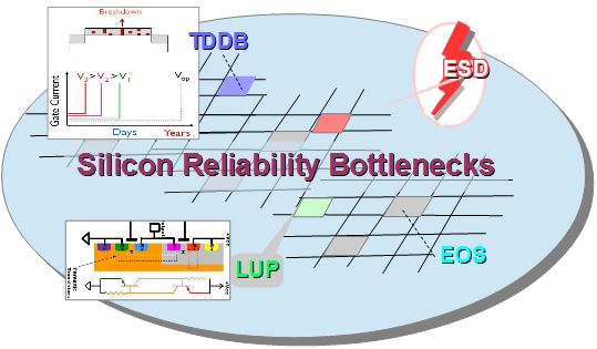
 Advanced process technology offers both device and interconnect scaling for increased design density and higher performance while invoking also significant implementation complexities. Aside from the performance, power and area (PPA) aspects, designer is getting entrenched with the need of tackling more reliability issues such as Electrostatic Discharge (ESD), Latch-Up (LUP) and Time-Dependent Dielectric Breakdown (TDDB). Traditionally these issues are observed during the cell library and technology development stage under as-designed operation voltage ranges. However, foundries or integrated device manufacturers (IDMs) are encouraging full-chip reliability verification to prevent chip reliability failures either during burn-in stage or in silicon.
Process and Reliability Design Rules
In the traditional RTL2GDS2 design flow, the standard cell library is initially targeted as the test vehicle for new process role-out as they are easier to be implemented compared with the other macro or custom blocks. Both timing and power attributes are normally captured in the library and synced-up with the foundry provided SPICE model version. Subsequently, the library could also embed process variations parameters through the Liberty Variation Format (LVF) extension.
During the 0.18 micron technology day, we were accustomed to the notion DFM (Design For Manufacturability). Since then, frequent collaborations between foundries and designers were taken place to minimize surprises from the manufacturing field. Designers would attempt to incorporate all known critical process parameters prior to tape-out. Foundry would provide PDK (Process Design Kit) and techfile releases early and maintain close-collaboration with customers’ technology and library teams to ensure proper adoption. Customer subsequently will pipe-clean and apply changes using foundry pre-approved reference flow.
Similar to PDK, a Reliability Design Kit (RDK) may be provided by foundries or IDMs, but with some critical design rules being presented as guidelines. For example, wire width threshold requirement is posted as criteria for nets in design to survive an ESD event. This rule can not be directly applied on the traditional DRC tool as it is lacking of the capability to identify electrical current directionality among others. In other examples, applying DRC driven approach to identify both LUP and TDDB is impractical as it has heavy reliance on using physical markers to identify polygons under analysis. This approach either does not work well at full-layout or may present loophole that deems it to be ineffective. Recent foundries/IDM proposed methodology is moving towards non-physical marker approach, allowing a more versatile logic-driven-layout (LDL) based checking. The combination of topological data and static design rules enable better reliability check coverage.
Calibre PERC and Reliability Bottlenecks
Mentor Calibre product family has been the industry leader for IC physical verification. Calibre PERC reliability platform provides complex reliability verification using both foundry’s standard rules and project custom rules. It employs topological constraints to verify correct circuit structures are in place as specified by circuit design rules. It has access and ability to concurrently use netist and layout information to perform electrical checks utilizing parameters in both domains.
The combination of Calibre PERL LDL flow along with static simulation and static voltage propagation features has enabled foundries and IDMs defining robust reliability rules. These rules can be implemented and automatically verified at full-chip ensuring a full coverage. Analogous to static timing approach used for resolving timing the latency and the scalability of dynamic-based circuit simulation, using the above approach cuts down the complexity and allows both block and full-chip reliability verifications.
Let’s review on how Calibre PERC utilizes static simulation and voltage propagation to address ESD, LUP and TBBD compliances.
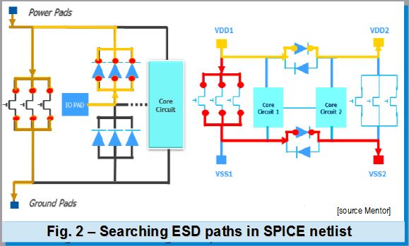
For ESD prevention, ESD or power clamping devices
(diode, transistor, resistor) with enough strength must be connected to IO, P/G and cross-power domain paths. As shown in figure 2, the types of checks Calibre performs on this type of condition include:
– Verify if the required circuits (ESD, power clamping, back-to-back diodes) exist.
– Check device parameters of the corresponding circuits have sufficient strength for ESD.
– Additional checks for for advanced nodes such as effective resistance and current density.
The second reliability issue is latch-up (LUP). IC’s LUP can be described as a short-circuit type event occuring in the parasitic-bipolar-pair equivalent structures and is triggered when disruptive excitation causes significant current or overcurrent looping in the positive feedback network (refer to figure 3a).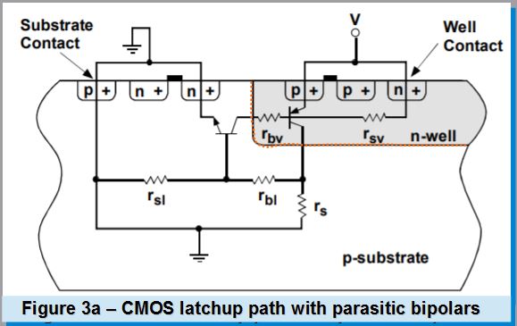
For a LUP prevention, the guard-ring or strap insertion is normally recommended. In addition, it requires the spacing among polygons involved with latchup (operate at different potentials) should be equal or larger than potential difference as shown in figure 3b. Calibre PERC handles LUP check by traversing 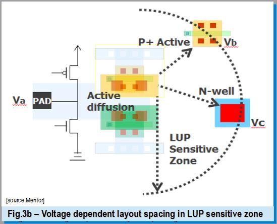 through extracted layout netlist and propagate
external voltage values into internal nets based on user-defined constraints. It has mechanism to annotate to physical polygons attributes to signify aggressor or victim devices and voltage value for DRC checks.
For interconnect TDDB checks on block or full-chip, spacing checks among polygons of the same layer but different nets are executed against criteria dependent on delta-voltage range. Voltage propagation of the external nets into the internal nets are done until all targeted nets for potential TDDB have the appropriate voltage values to annotate to the corresponding polygons. 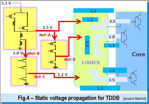 Designer could apply constraint to control the static voltage propagation across multi voltage domains. For example, in static propagation shown in figure 4: the top port has a 3.3 v while nets A, B, C can be assigned with voltage 2.5v, 1.8v and 2.2v, respectively. A voltage shift is done by user-defined subcircuit pattern or through simulation. Subsequent static voltage propagation is done, followed by annotation of the voltage values to polygons in nets of concern for DRC checking.
Increased reliability issues stemming from the advanced process technologies are introducing additional complex sign-off requirements as they are not easily resolved and scaled through the use of dynamic simulation or traditional DRC checks. Such limitation is no longer the case with the availability of Mentor Calibre PERC reliability platform. It has both capacity and fast performance to allow an accurate full-chip verification for a full design-for-reliability (DFR) compliance. For more detailed discussions on Mentor PERC related to solving reliability issues, check this LINK.
Share this post via:


Comments
There are no comments yet.
You must register or log in to view/post comments.