RVN! 26 Banner revised (800 x 100 px) (600 x 100 px)

Podcast EP31: Interview with Dr. Rosemary Francis, Chief Scientist at Altair

Podcast EP31: Interview with Dr. Rosemary Francis, Chief Scientist at Altair
by Daniel Nenni on 07-30-2021 at 10:00 am

Dan is joined by Dr. Rosemary Francis. Rosemary was the managing director and CEO of Ellexus Ltd. before its acquisition by Altair. Dan explores the I/O profiling technology Ellexus brought to Altair, it’s impact and the implications for the future. A behind-the-scenes view of the acquisition is also provided.

Dr. Rosemary Francis founded Ellexus in 2010, which was acquired by Altair in 2020. She obtained her PhD in computer architecture from the University of Cambridge and founded Ellexus to build tools for managing the complex tool chains needed for semiconductor design. Ellexus went on to become the I/O profiling company, working with high-performance computing organizations around the world in semiconductor, life sciences, and oil and gas. Now part of Altair, Francis continues to lead the Ellexus team to work on job-level analytics and storage-aware scheduling. She is a member of the Raspberry Pi Foundation, an educational charity that promotes access to technology education and digital making.

The views, thoughts, and opinions expressed in these podcasts belong solely to the speaker, and not to the speaker’s employer, organization, committee or any other group or individual.


Highlights of the “Intel Accelerated” Roadmap Presentation

Highlights of the “Intel Accelerated” Roadmap Presentation
by Tom Dillinger on 07-30-2021 at 6:00 am

ribbon FETs

Introduction

Intel recently provided a detailed silicon process and advanced packaging technology roadmap presentation, entitled “Intel Accelerated”.  The roadmap timeline extended out to 2024, with discussions of Intel client, data center, and GPU product releases, and especially, the underlying technologies to be incorporated into those products.

This article will focus on the technology roadmaps, rather than the “Lake” (client) and “Rapids” (data center) product families, such as Meteor Lake, Sapphire Rapids, and Granite Rapids.  Also, look for an upcoming article on how the Intel Foundry Services (IFS) initiative will also be leveraging these technology introductions.

Scott Jones published a comprehensive SemiWiki article summarizing the revised silicon process nomenclature that Intel will be adopting – link.

Personally, of all the criteria used to evaluate a silicon process for a potential product design – e.g., performance per watt, circuit/SRAM density, IP availability, low power options, cost, qualification at environmental corners, lifetime reliability – the actual process node name is not one of them.  Nevertheless, Intel has updated their process nomenclature to “sorta” align with other foundry naming conventions.  The timeline for these process node introductions is discussed next.

5 Nodes in 4 Years

Pat Gelsinger, Intel CEO, described the process technology (and Intel CPU) roadmap in the following manner, “We will continue the model of micro-architecture development and process introduction, but at a torrid pace.  The spirit of the Tick-Tock release model is alive, but with focus on more parallel innovation.  We will de-risk new technology introductions.  Proven micro-architectures will be transitioned to new process nodes.  As an example, the upcoming backside power distribution technology will be proven using the I3 technology node before introducing into high volume manufacturing with the I20A node.  Also, the requisite capital equipment and staffing requirements for this roadmap are fully funded.”

Note that the process descriptions that were provided focused on “performance per watt” (more on that later), as opposed to circuit density scaling.  Here is the silicon process roadmap:

10 SuperFin (10SF)

  • currently in volume production,
  • “the most significant intra-node performance improvement (over 10+) in Intel’s history”

I7 (was originally denoted as “10 Enhanced SuperFin”)

  • +10-15% performance per watt gains over 10SF
  • increased device channel strain
  • Alder Lake (big/little X86 core mix) available late 2021, Sapphire Rapids available 1Q22

I4

  • +20% performance per watt improvement over I7
  • first introduction of EUV lithography
  • ramp in 2H22, high volume manufacturing in 2023 (Meteor Lake, Granite Rapids)

I3

  • +18% performance per watt compared to I4  (FinFET-based)
  • new high-performance library
  • improved transistor drive current
  • improved BEOL characteristics (e.g., reduced via resistance)
  • increased EUV deployment
  • ramp in 2H2023, HVM in 2024
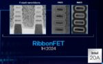
I20A

  • ramp in 1H2024
  • transition to “ribbon FET” (gate-all-around) device topology
  • introduction of backside power delivery

I18A

  • ramp in 1H2025

Although there is some flexibility in the definition of process introduction “ramp” compared to high volume manufacturing, the timeline for this roadmap is indeed extremely aggressive.

As mentioned above, the focus of the process roadmap discussion was to highlight the performance-per-watt comparisons between nodes.

I had the opportunity to chat briefly with Sanjay Natarajan, Senior VP and co-General Manager for Logic Technology Development, who indicated, “We have the line of sight in place to realize this process roadmap.”  I asked Sanjay about the performance per watt improvement targets.  He replied, “This is a result of a comprehensive analysis across a broad suite of designs – from ring oscillators and cell libraries to large building blocks and cores in a product-like environment.  These improvements are from many process optimizations – not just transistor drive current, but also throughout the interconnect stack, including power delivery.” 

EUV

Intel has been conservative in their deployment of (0.33NA) extreme ultra-violet lithography, and their assessment of the cost/yield tradeoffs between EUV and DUV multipatterning litho.

As described above (and summarized in Scott’s article), process node I4 will be the first to incorporate (limited) EUV mask layers in 2H2022, with greater adoption in node I3 (2H2023).

Dr. Ann Kelleher, Senior VP and General Manager, Technology Development, highlighted, “The four pillars of EUV lithography have achieved manufacturing maturity – photoresist, masks, pellicles, and metrology.” 

Ann also mentioned that Intel anticipates being the first to incorporate (0.55NA) “high NA” EUV lithography (for the I18A node), as a result of their collaboration with ASML.  (For more info on the challenges of high NA EUV photoresist development, here is an earlier SemiWiki article from Intel R&D – link.)

GAA

As mentioned above, node I20A incorporates a transition from FinFET devices to a gate-all-around configuration, denoted by Intel as “ribbon FETs”, illustrated below.

(A cynical engineer would observe that there are several different names being used for the GAA device – so much for nomenclature consolidation in the industry.)

The figure above shows 4 stacked device channels surrounded by the gate – clearly, a performance-oriented implementation.  Researchers are actively evaluating the “optimum” number of stacked channels, as well as the minimum/maximum channel width design flexibility;  there is also active research to evaluate the process complexity and yield impact of locally removing channel(s) from the stack for circuit applications that would leverage lower device drive current (at minimum width).

Backside Power Delivery and “Power Vias”

Intel showed die cross-sections of backside power delivery metallization, utilizing “power vias” – the target node is I20A, concurrent with the ribbon FET introduction.

Sanjay indicated, “There are significant benefits to both improved signal routing track availability and reduced power distribution network losses with backside power delivery.  There are challenges, as well, working with the thinned wafer substrate.  We have broad expertise across both silicon and packaging technology development groups, for the requisite grinding, etch, and fill steps.” 

Sanjay added, “The power via strategy provides full connectivity to the circuitry fundamental to power state management of the PDN.” 

IDM 2.0 and IFS

Pat G. also clarified the company strategy with regards to the Integrated Device Manufacture (IDM2.0) business model, and the renewed emphasis on providing foundry services.

  • “We will continue to manufacture the majority of our products internally, with some outsourcing.  We are making considerable investments in expanding and updating fabs in Oregon, Arizona, and Israel (silicon), as well as in New Mexico (advanced packaging).”
  • “These advanced process nodes will be available to IFS customers.”  (Intel announced an IFS collaboration with Qualcomm, focused on the I20A node.)

Packaging Roadmap

Intel’s advanced packaging investments will continue evolutionary enhancements to their 2.5D and 3D offering, to optimize multi-die integration and die interface bandwidth.

EMIB

The Embedded Multi-die Interconnect Bridge (EMIB) provides for 2.5D package interconnections between die, introduced by Intel in 2017.  it utilizes a dense pitch microbump connection between the die edges and a silicon “bridge”, as shown below.  (also, a previous SemiWiki article link)

There is a significant cost benefit compared to a full-size silicon interposer, especially considering the increased number of die (and die stacks) integrated into the final package, which requires >1X maximum silicon lithography reticle size.  As an example, Sapphire Rapids will be a 92mm x 92mm BGA package.  (Wow.)

The EMIB microbump pitch roadmap depicts a transition from 55um to 45um (used on Sapphire Rapids) to 40um.

Foveros

Intel’s 3D stacked die technology is denoted as Foveros.  As illustrated in the figures below, Foveros encompasses two configurations – a microbump-based die attach technology, and a direct hybrid bonded connection.

The second generation microbump Foveros technology, denoted as Foveros-Omni, introduces a 36um microbump pitch.  The upcoming Meteor Lake product family announcement in process node I4 will showcase the Foveros-Omni offering.

The roadmap presented suggests a subsequent microbump pitch of 25um.  Through silicon vias and through package copper columns complete the overall package interconnect offering.

Pat G. indicated, “Foveros-Omni offers an attractive cost-performance-power benefit (compared to EMIB) for client products in the mobile markets.”  

Foveros-Direct is the hybrid bonded package designation, to be released in 2023.

I had a chance to chat briefly with Dr. Babak Sabi, VP and General Manager of the Assembly and Test Technology Development group, about the EMIB and Foveros packaging strategy.  He indicated, “The Foveros-Direct introduction will utilize a ‘sub-10um’ hybrid bond pitch, offering an exceptional die-to-die connectivity density.  (~10K/mm**2)  Our assembly and test technology team is implementing improved die sort technologies for the known-good die integrated into these packages.” 

Babak added, “Further, the EMIB and Foveros technologies are complementary.  An example of a combined EMIB and Foveros implementation is the upcoming Ponte Vecchio GPU.”

I asked Babak about some of the challenges in the development of these packaging technologies.  He replied, “For Foveros-Omni, mechanical alignment of the stacked die is a challenge, especially as we look to scale the bump pitch below 25um, to the 15-20um range.  Another big issue is to have clean die edges after separation – you need to have no particulates introduced during the assembly process.  And, we are working closely with EDA tool providers on signal integrity and power distribution network modeling and simulation, and especially on the thermal-mechanical analysis of the entire assembly.  These complex packages need to be correct-by-construction.”

Futures

  • Intel’s Innovation Event will be a (hybrid) conference in San Francisco on October 27-28 (likely including the Alder Lake client CPU announcement).
  • According to Pat G., expect an announcement on fab expansion “by year end”.  (This was mentioned in the context of Intel’s support for US and EU government support for increased domestic fabrication.)
  • Process node I18A was mentioned briefly, targeting initial availability in 1H2025.
  • Intel has been investing significantly in (integrated) silicon photonics circuitry, for optimized interface bandwidth and “picoJoules per bit” power dissipation.

Summary

Intel has clearly re-focused their considerable expertise in materials, lithography, and device technologies.  They have presented an aggressive silicon and packaging technology roadmap – especially noteworthy is the cadence of new process introductions (and, significantly, to offer these technologies to IFS customers, as well).

As far as the execution of this roadmap, Sanjay’s quote of confidence is especially noteworthy,  “We have line-of-sight into these innovations.”

(Personally, I’ll reserve judgment on the high NA EUV rollout, but that’s not expected until 2025.)

Interesting times, indeed.

-chipguy


Cerebrus, the ML-based Intelligent Chip Explorer from Cadence

Cerebrus, the ML-based Intelligent Chip Explorer from Cadence
by Kalar Rajendiran on 07-29-2021 at 10:00 am

Screen Shot 2021 07 21 at 4.39.06 PM

Electronic design automation (EDA) has come a long way from its beginnings. It has enabled chip engineers from specifying designs directly in layout format during the early days to today’s capture in RTL format. Every advance in EDA has made the task of designing a chip easier and increased the design team productivity, enabling companies to get their products to market quicker. Of course, the product requirements have not been staying static during this time. So, it has been a tug-of-war between EDA advances and design complexity increases.

One thing that has remained constant in the chip world is the desire for a tool that will take in design specifications and product constraints and with the push of a button, generate a design that is manufacturable, production ready and meets or beats the stated product constraints. It is a lofty goal indeed. Last week, Cadence announced the Cerebrus Intelligent Chip Explorer. It is a machine learning (ML)-based tool that takes the chip world one step closer in that direction. It delivers enhanced PPA, higher team productivity and shorter time to market benefits for its customers.

During CadenceLIVE Americas conference in June, Cadence mentioned a number of areas where it has been incorporating ML technology, and Cerebrus is the latest result of Cadence’s ML initiative. I expect to hear more product announcements resulting from the ML initiative.

I had an opportunity to discuss the Cerebrus announcement with Kam Kittrell, senior product management group director in the Digital & Signoff Group at Cadence. The following is a synthesis of what I gathered from my conversation.

What is Cerebrus?

It is a new type of EDA tool from Cadence that works with the RTL to GDS signoff flow. It takes power, performance and area targets for a design or a block within a design. The user can provide a start and end point of the flow or tell the tool to do the full flow. The tool works within the context of the standard production flow that includes multiple tools and IP blocks and also accommodates personal configuration preferences of the respective CAD team running this tool. It is an automated RTL-to-GDS full flow optimization tool.

Although EDA stands for automation, until this point in time, learnings from past designs were not automatically fed into newer design flows. Cerebrus not only uses ML to explore better designs but also saves learnings for leveraging into new designs.

Why is Cerebrus Needed?

One could be thinking, EDA tools that I am familiar with are pretty good. The tools already do a great job. Once I get a design to a basic working status, squeezing the last ounce of performance or power savings or area savings is the task of expert engineers. While that is how things have been done historically, we know that optimization efforts consume lot of engineers, time and compute resources. Cerebrus on the other hand can run 50 to 100 different experiments very quickly. In essence, by leveraging ML techniques, it can search a much larger space in far less time than is possible via manual means and arrive at the optimal path for reaching the goal.

Refer to figure below. It shows benchmark results from a 5nm mobile CPU design.

After taking this design to a working status using a basic flow, many engineers worked over several months to achieve a flow that delivered the PPA goal for the design. In parallel, Cerebrus took off from the basic starting point and kicked off the investigation to find the optimal path. The objective of this benchmarking exercise was to increase productivity without compromising on PPA goals. Cerebrus achieved the goal in much less time using the same amount of compute resources and using just one engineer and ended up improving the PPA as well, automatically.

How does Cerebrus Work?

Automation is all about achieving efficiencies. EDA increases people productivity in achieving design goals. Through ML techniques, Cerebrus helps increase EDA flow efficiencies and enables tools to quickly converge on better placement and route and timing closure. ML types of applications usually require lots of training before a model can be developed and used. And the training phase requires lot of compute resources.

But Cerebrus does not need a large training set before it can start working. And it does not need a large compute farm either. With no training on a particular process node, it can find an optimal path quickly. The resulting model can be reused on the same design for further refinements. The model can also be transported to a different design with similar operating conditions and same process node as the earlier design. The reinforcing nature of Cerebrus’ learning model increases effectiveness with each use. Result is significant PPA improvements, resource optimizations (people and hardware) and schedule compressions.

Scalable, Distributed Computing Solution

Cerebrus just takes one engineer to manage the automated RTL-to-GDS flow optimization runs for many blocks concurrently, allowing full design teams to be more productive.

Cerebrus supports all leading cloud platforms. With a manual approach to PPA refinement, typically on-demand compute resources are locked in for a long period of time, whereas with Cerebrus’ ML-based automated approach, on-demand compute capacity is kept for a much shorter period of time to arrive at the optimal path. In this sense, it provides more efficient on-site and cloud compute resource management than the traditional human-driven design exploration.

When is Cerebrus Available?

It is in general availability (GA) now.

Some Interesting Use Cases for Cerebrus

In addition to the standard use case where PPA optimization or productivity improvement is the objective for using Cerebrus, there may be situations that trigger different use cases.

  • Customers sometimes think of a derivative product when working on the primary product and decide to arrive at a product that is in-between because they think they cannot do both chips. Alternately, they may decide to build a superset of a chip and turn off portions of the chip to deliver a derivative product. Neither of these paths are ideal. Cerebrus can help customers do both chips in parallel with fewer engineers (smaller team) than what would otherwise be needed and achieve both chips that are optimized for their purposes.
  • Refer to figure below which shows the results from an exercise for optimizing floorplan and implementation plan concurrently.

Summary

The revolutionary ML-based Cerebrus enables customers to meet increasingly stringent PPA, productivity and time-to-market demands of their respective market segments. Cerebrus also makes it easier and quicker to develop optimized chip derivatives. The press announcement can be found here and more details can be accessed in the product section of Cadence website. You may want to discuss with Cadence and explore incorporating Cerebrus into your chip design flow.

Also Read

Instrumenting Post-Silicon Validation. Innovation in Verification

EDA Flows for 3D Die Integration

Neural Nets and CR Testing. Innovation in Verification


SoC Vulnerabilities

SoC Vulnerabilities
by Daniel Payne on 07-29-2021 at 6:00 am

side channel attack

As I read both the popular and technical press each week I often see articles about computer systems being hacked, and here’s just a few vulnerabilities from this week:

Here on SemiWiki we have many engineers responsible for SoC hardware, software, firmware and security, so what are the best practices to make your new or existing electronic systems more hardened against attacks, and less vulnerable?

Gajinder Panesar and Tim Ramsdale are two experts from Siemens EDA and Agile Analog, respectively, and they teamed up to write a 15 page White Paper, “The Evolving Landscape of SoC vulnerabilities and analog threats.” I’ll share the gist of what I learned from reading this.

Vulnerabilities

One security premise is that relying only on software updates to patch vulnerabilities is not sufficient, so adding security as part of the hardware design should be considered. There’s even an Open source project called OpenTitan, to help you build a transparent, high-quality reference design and integration guidelines for silicon root of trust (RoT) chips. With a hardware-based RoT, only firmware compared against a known signature can be run, stopping attempts to load any hacked firmware.

Hackers are becoming creative and resourceful enough to examine the secret keys in an RSA algorithm by making hardware measurements, noting small variations in how operations are executed, aka side-channel attack. Shown below are four multiplication portions by the purple arrows, then the negative spikes are part of the squaring and modular reduction in the algorithm.

Side-channel attack

Security clues can be revealed by examining several things:

  • Cache activity
  • Execution pipelines
  • Electromagnetic (EM) values
  • Voltage variations
  • Current variations

Another example of a side-channel attack has the hacker trying to guess one of the key bytes, and around region 350 they found one correct key byte.

Attack output vs sample number for subkey guess

Targets for hacking include 5G infrastructure, edge servers, IoT devices, cloud computing, autonomous vehicles, industrial robotics. Hackers are using statistical approaches to measure electronic devices, providing clues to security vulnerabilities.  One counter-measure is for the hardware design team to add random electrical noise.

Another technique that hackers use is to intentionally glitch the power supply at a specific time point, which can then flip a stored bit into an unsafe state, as documented by German security company LevelDown. Even some older processors had an exploit where a hacker used illegal opcodes, which in turn put the processor into a vulnerable state.

Temperature is yet another technique where an attacker can run a SoC at a higher or lower temperature than specified, in order to alter the internal state or even extract private keys from a physically unclonable function (PUF).

An attacker may use voltage changes to the supply rail, in order to slow down or speed up the logic, causing internal bits to flip, and illegal states to be reached.

If a hacker has physical access to your electronic system, them directly controlling the clock inputs by changing the duty cycle, or introducing glitches will change the internal logic. ChipWhisperer is a company with an open-source system to expose weaknesses from embedded systems, using side-channel power analysis and fault injection.

ChipWhisperer

Fault injection using electromagnetic (EM) radiation is a technique used by ChipShouter, but they would have to be precisely timed with internal clock edges to create a repeatable fault. Even using a laser light on a de-capped IC package can force internal errors for an SoC.

Countermeasures to Vulnerabilities

  • Clock glitches: Internally generated source for comparison.
  • Power glitches: Brownout detectors
  • Temperature attack: Temperature sensors

At Siemens EDA they offer a product called Tessent Embedded Analytics, and it embeds hardware monitors in your SoC, then communicates with a message-based architecture. Adding hardware security IP from Agile Analog provides checks on clock, voltage and temperature:

Monitors from Agile Analog

These monitors can sense an exploit, then the embedded analytics can both report and decide the appropriate security response. The combination of embedded analytics and security IP shown in a diagram:

Embedded analytics and security IP

Summary

The great power and benefits of SoC design are under attack from hackers, so it is up to the design community to adopt pro-active measures to harden the security level of their new products. What Siemens EDA and Agile Analog have created is a framework of embedded digital and analog hardware, to enable detection of cyber threats, and a means to take appropriate action, in real time.

Yes, this means more work for your design team, but your customers will place a higher value on a more secure SoC. You don’t have to start from scratch either, because Siemens EDA and Agile Analog have done the ground work for you.

To read the full 15 page White Paper, visit this page and provide a few details about yourself.

Related Blogs


Optimize RTL and Software with Fast Power Verification Results for Billion-Gate Designs

Optimize RTL and Software with Fast Power Verification Results for Billion-Gate Designs
by Johannes Stahl on 07-28-2021 at 10:00 am

ZeBu Empower diagram

In every chip, power is a progressive problem to be solved. Designers have long had to rely on a combination of experience and knowledge to tackle this dilemma, typically having to wait until after silicon availability to perform power analysis with realistic software workloads. However, this is too late in the game, as it becomes a costly and time-consuming proposition to resolve power issues post-silicon. In this blog post, I’ll explain how you can achieve actionable power verification results in hours on billion-gate designs early on. With this capability, you can find the critical regions and time windows for peak power and, thus, optimize your RTL and software.

Performing power analysis post-silicon introduces the risk of missing critical high-power situations, which can create significant cost and product adoption problems. The downsides of being wrong about power? A customer could opt to go with another chip vendor if a design misses the promised power target. Or, a system designer might be forced to dial back chip performance to maintain the targeted power envelope—an unfavorable tradeoff in applications that rely on fast compute performance. In this post, which was originally published on the “From Silicon to Software” blog, we’ll take a closer look at some SoC application areas where accurate power analysis is essential.

GPUs

Traditional GPU applications are known entities by comparison, but this doesn’t make the power analysis task any easier. Consider a GPU designed for a laptop computer. You can run power analysis at certain measurement points over a period of time. However, with potentially up to 10 million clock cycles, this approach is clearly not exhaustive—which is why designers traditionally have had to rely on their best estimates for power.

Artificial Intelligence

In artificial intelligence (AI) chips, the applications as well as the software stack for AI applications and architectures are all new territory, which poses more challenges from a power profiling perspective. Yet, the potential rewards of optimizing AI applications for power are great. Power efficiency, after all, is an advantage that AI chip designers would love to be able to tout, along with fast compute performance.

5G

Another power-critical application is 5G, which is all about high performance and low latency. 5G applications involve a lot of parallel processing and high frequencies, but, with only so much power available, they must be optimized to run efficiently. This is particularly true for radio head chips.

Data Centers

Data centers, especially hyperscale data centers, are built on lightning-fast, energy-efficient chips that can help maximize total system throughput. With billions of gates along with complex software workloads, data center SoCs come with particularly demanding verification and software bring-up requirements.

Mobile

Given their compact form factor and desired long battery life, mobile devices such as smartphones cannot afford to use chips that consume too much power. While their workloads have grown in complexity, these devices—even the power-hungry GPUs—must still be able to accommodate these workloads power efficiently.

How a Fast Power Emulator Solves the Power Profiling Challenge

As meeting dynamic power requirements becomes increasingly difficult, chip designers often consider power to be their top verification challenge. Dynamic power verification requires finding peak power. Yet, critical peak power events are driven by actual software workloads. Simulation can identify peak power that falls above as well as below the power budget, but in billion-gate designs, it will only be able to catch the real critical events by pure luck, as the windows a simulation based approach can consider are much too small. A signoff tool would provide accurate power measurements, but if it is used on the wrong time window, the designer would not be able to determine which window has the highest power.

Identifying low-power bugs requires running software workloads. Small tests won’t expose realistic workload-driven power bugs. What’s needed is:

  • Real firmware and operating system at pre-silicon testing
  • Emulation to verify power over millions or billions of cycles
  • Pre-silicon power verification for debug, which isn’t possible with actual silicon

High-speed emulation allows design teams to perform power verification earlier in the design cycle, so they can minimize the risks of power bugs and missed SoC power goals. Indeed, a fast power emulator can be the answer to the hardware/software power verification dilemma, providing better accuracy across a broader window. The ideal emulator would be able to run multiple iterations a day on large designs with realistic workloads. By doing so, chip designers can gain actionable insights into the power profile of their designs.

Actionable Insights in Hours

With multi-billion-gate SoC workloads in mind, Synopsys has unveiled its new Synopsys ZeBu® Empower emulation system for hardware/software power verification. Delivering maximum compute performance, ZeBu Empower can perform multiple iterations a day, providing actionable results in hours. Based on the resulting power profiles, hardware and software designers can, early on, identify areas where they can improve dynamic and leakage power. ZeBu Empower utilizes ZeBu Server fast emulation hardware technology to provide the short turnaround times.

ZeBu Empower also feeds forward power-critical blocks and time windows into the Synopsys PrimePower engine to accelerate RTL power analysis and gate-level power signoff. Both ZeBu Empower and PrimePower are part of the Synopsys software-driven low-power solution. Pictured in the diagram below, the low-power solution provides an end-to-end flow and methodology spanning from architecture analysis to block RTL power analysis to SoC power analysis and optimization.

The Synopsys software-driven low-power solution is designed to help reduce overall dynamic and static power consumption of ICs.


Summary

Power might just be the most challenging part of the power, performance, and area (PPA) equation. And when it comes to multi-billion-gate designs, the complexity in achieving accurate power profiles only grows. However, with the fast power emulation solution from Synopsys, designs teams can now find the critical regions and time windows for peak power, so they can optimize their RTL and their software. By taking advantage of the comprehensive Synopsys low-power flow, designers gain tools that can help them meet their PPA targets. Given the heavy workloads and performance demands of applications like GPUs, AI, 5G, data centers, and mobile, any solution that can provide a more accurate power picture should be a welcome addition to any designer’s PPA toolkit.

Also Read:

Driving PPA Optimization Across the Cubic Space of 3D IC Silicon Stacks

Die-to-Die Connections Crucial for SOCs built with Chiplets

Mars Perseverance Rover Features First Zoom Lens in Deep Space


Instrumenting Post-Silicon Validation. Innovation in Verification

Instrumenting Post-Silicon Validation. Innovation in Verification
by Bernard Murphy on 07-28-2021 at 6:00 am

Instrumenting Post-Silicon Validation

Instrumenting post-silicon validation is not a new idea but here’s a twist. Using (pre-silicon) emulation to choose debug observation structures to instrument in-silicon. Paul Cunningham (GM, Verification at Cadence), Raúl Camposano (Silicon Catalyst, entrepreneur, former Synopsys CTO) and I continue our series on research ideas. As always, feedback welcome.

The Innovation

This month’s pick is Emulation Infrastructure for the Evaluation of Hardware Assertions for Post-Silicon Validation. The paper was presented at the 2017 IEEE Transactions on VLSI. The authors are from McMaster University, Hamilton, ON, Canada

The authors distinguish between logical and electrical errors post-silicon and devote their attention in this paper to electrical errors, detectable through bit-flips in flops. Their approach is to determine an optimal set of assertions in pre-silicon analysis. These they then implement in silicon in support of post-silicon debug. The pre-silicon analysis is similar to faulting in safety analyses, injecting faults on flops corresponding to electrical errors, as they hint in the paper. They generate a candidate list of assertions using assertion synthesis; the core of their innovation is to provide a method to grade these assertions by how effective each is in detecting multiple faults.

Input generation is random, analyzing injected faults (treated as transient)  in sequence. They allow a user-specified number of cycles for detection per fault. In a subsequent phase, they measure effectiveness using two different coverage techniques. For flip-flop coverage, they count an assertion if it catches an injected error on any flop. In bit-flip coverage, they score assertions number of errors detected on separate flops. These metrics, together with area estimates, they use (alternately) to select which preferred assertions.

Paul’s view

This paper pairs nicely with our August 2020 blog on quick error detection (QED). QED accelerates post-silicon functional bug detection, where this blog focuses on post-silicon electrical bug detection. The paper is an easy read, although it helps to first read reference [23].

Electrical bugs are hard to catch, and even then, are hard to replicate and find the underlying physical cause. The authors propose a method, through embedded logic, to detect when such bugs cause a flop to flip to an incorrect value (they don’t dig deeper than finding these flips).

The heart of the paper and its companion reference [23] is a multi-step method to create and synthesize this detection logic. It begins with mining properties of the design as temporal assertions using the GoldMine tool. They rank assertions based an estimate of their ability to detect bit flips, and an estimate of the area / wiring cost to implement in silicon. Ranking relies on running many pre-silicon simulations with candidate assertions, injecting bit flip errors and counting detected flips by assertions. In the original paper they used logic simulation, here they accelerate these simulations by mapping the design to an Altera FPGA board.

I like how they pull together several innovations into a coherent method for post-silicon bit flip detection: assertion mining, assertion synthesis, and an elegant ranking function for assertion selection. However, the results section of the paper indicates that detecting bit flips in n% of the flip-flops requires roughly an n% increase in design area. This seems challenging for commercial application, especially since it only helps find electrical bugs. One could potentially achieve a similar  result by cloning the logic-cone driving a flip-flop, then compare the output of this cloned logic to the original logic. This would seem to generate a similar area overhead as their method, in the limit cloning the entire design (i.e. 100% area overhead) to detect flips in 100%  of the flops in the design.

Raúl’s view

The paper is self-contained with a fair amount of detail. The authors ran experiments for 3 ISCAS sequential circuits (approx. 12K gates, 2000 FF). Preparation experiments inject 256 errors per flip flop and using all assertions generated by GoldMine. Due to the limited capacity of the FPGA the authors split runs unto 45 “sessions” for one circuit. The results show, even with 45 sessions, an acceleration in analysis over simulation of 20-500 times (only up to 8 error injections because simulation gets too slow, 105h). The maximum achievable Flip-Flop coverage is 55%, 89% and 99% for the 3 circuits. The number of assertions mined controls coverage.

Running with selected assertions (corresponding to a 5-50% area overhead) and 1-256 injections results in 2.2%-34% bit coverage. Most of the time, the assertion miner ran for 228h. One thing that confused me is their data for run-times versus errors injected. The increase looks reasonable (linear) in simulation. But in emulation it jumps massively, from 0.045h to 5.4h for an increase of 2 to 8 error injections. I’d like more explanation on this point.

This is a methodology paper. I like that pretty much every step can be substituted by a commercial tool. Together with using a large FPGA board (as emulator) the methodology scales. Methodologies are of course very hard to commercialize, but it’s a nice application for existing technology!

My view

The method of exploring a safety analysis technique for post-silicon debug is intriguing. A novel idea, even though leading to a somewhat impractical result for commercial application.

Also Read

EDA Flows for 3D Die Integration

Neural Nets and CR Testing. Innovation in Verification

Circuit Simulation Challenges to Design the Xilinx Versal ACAP


EDA in the Cloud – Now More Than Ever

EDA in the Cloud – Now More Than Ever
by Kalar Rajendiran on 07-27-2021 at 10:00 am

Screen Shot 2021 07 14 at 4.32.16 PM

A decade ago, many of us heard commentaries on how entrepreneurs were turned down by venture capitalists for not including a cloud strategy in their business plan, no matter what the core business was. Humorous punchlines such as, “It’s cloudy without any clouds” and “Add some cloud to your strategy and your future will be bright and sunny” were common.

Fast forward to now and there is no denying that cloud computing is well established across most industries. From on-prem computing resources being sufficient, conditions have changed to make on-cloud computing a necessity for almost everyone.

It’s true that early interest for EDA to move to the cloud was soft. Quite a lot has changed over the last decade. But there are still companies out there that are evaluating EDA in the cloud. This is the backdrop for a recently published whitepaper. It was authored by Michael White, senior director, physical verification product management, Calibre Design Solutions at Siemens EDA.

The whitepaper covers the history of EDA in the cloud, why the cloud became a viable option for EDA, and identifies ways for improving the bottom line for designs in both established nodes and leading-edge technologies. This blog covers the salient points I gleaned from the whitepaper.

Paving the Way

There were two primary reasons for EDA’s early hesitancy to move to the cloud. The significant reason was the deep concern over intellectual property (IP) security. The other reason was that there was no compelling need as the on-prem computing resources were able to handle all of the requirements.

Cloud providers took the IP security concern seriously. They started investing in and developing strong security mechanisms in their infrastructure and deploying tight security protocols and procedures for data access and during data transportation. With this intense focus on IP security by cloud providers, the chip industry started migrating to cloud computing.

Compute Demand Growth

The demand for EDA compute power has been growing aggressively over time. As we advanced from one process node to the next, the number of rule checks that needs to be performed also increased. Refer to figure below. From 28nm to 5nm node, the number of rule checks has quadrupled. In addition, each task has also increased in complexity. For example, to optimize yield ramp, it is no longer simply adding in a few geometries. Design companies are trying to maximize yield using techniques such as cell-based fill.


The industry had hoped that innovations in lithography and transistors would bring down the amount of compute requirement by eliminating some of the rule checks that were added over the years. But that does not appear to be having a material impact on the long-term demand for compute power. And neither is the move toward chiplets integration (vs very large and complex SoC) expected to provide that much relief in regard to demand for compute power.

On-prem, Cloud or Hybrid?

Cloud computing can be more expensive than utilizing on-prem compute resources. To cost-effectively utilize cloud computing resources without sacrificing on turnaround times, there are many tools out there. Refer to one of my recent blogs for one such solution. But first start with how effectively current on-prem compute resources are being utilized. If utilization is low, first order of business is to improve the resource allocation and scheduling processes. If utilization is high without impacting project schedules, on-prem computing may be fine for current projects.

But even if the on-prem resources have been optimally planned, all it takes is for one or a few of the many projects to slip their schedules. Suddenly the situation changes from on-prem resources being sufficient to on-cloud computing becoming a necessity. May be in the form of hybrid computing environment. But what about the immediate future? Even moving an existing design to a new process node will increase the demand on compute power, making extending to the cloud a serious consideration. Refer to figure below.

Even if the above issues aren’t there, a company has to look at the market value for doing things faster than otherwise possible. What is the bottom-line benefit of tapping into the practically near-infinite cloud resources to get the company’s product faster to market.

Calibre Platform and Cloud Computing

Michael describes how their Calibre platform has been supporting distributed and cloud computing for more than a decade. Calibre engines and licensing can deliver the same level of performance whether a company is using a private cloud or a public cloud. Calibre engines can scale up to 10K+ CPU cores and process extremely large (GB to TB sized) files.

The whitepaper provides a specific example of how Advanced Micro Devices (AMD) was able to double their daily DRC iterations on a 7nm production design without increasing the memory usage on the cloud servers. He also describes how Siemens EDA was able to achieve a 30% further reduction in runtime by identifying optimizations to AMD’s runtime environment, Microsoft Azure’s cloud resources and the foundry’s design rule decks. You can find more details in the whitepaper.

Siemens EDA offers its customers flexibility to use the cloud for surge compute demand and continued use of multi-vendor flows. As part of that freedom of choice focus, they collaborate with multiple companies to create best practices for efficiently and cost-effectively utilizing the cloud. In this context, another blog that may be of interest is “Library Characterization: A Siemens Cloud Solution using AWS.”

Summary

If you have not already moved to the cloud for your EDA computing needs, it may be worthwhile to revisit that choice. After evaluating and making the decision to adopt cloud EDA computing, availability of proven technology, flexible use models, support for multi-vendor flow and guidance through best practices methodology are imperative to maximize the benefits received. Click here to download the whitepaper and explore with Siemens EDA.


Intel Accelerated

Intel Accelerated
by Scotten Jones on 07-27-2021 at 6:00 am

Intel Process Name Decoder

Intel presented yesterday on their plans for process technology and packaging over the next several years. This was the most detailed roadmap Intel has ever laid out. In this write up I will analyze Intel’s process announcement and how they match up with their competitors.

10nm Super Fin (SF)

10nm is now in volume production in three fabs located in Arizona, Israel, and Oregon. 10nm wafer volume has now crossed over and is higher than 14nm wafer volume, marking true high volume production. 10nm Super Fin was formally known as 10+.

7nm

Not to be confused with Intel’s former 7nm process, this is a rename of the 10nm Enhanced Super Fin process and offers a 10-15% performance improvement over 10SF. This should provide better performance than TSMC 7nm (performance similar to 10SF), but not as good as TSMC 5nm. Intel’s 10nm process offers roughly 100 million transistors per millimeter squared (MTX/mm2) so this process is competitive in density to Samsung and TSMC 7nm processes that are also around 100MTx/mm2.

The performance improvement is due to more transistor channel strain, lower resistance, more metal layers, and improved patterning techniques. This is entirely speculative on my part, but the “improved patterning technique” statement taken with the 4nm description as “Fully Embracing EUV” makes me wonder if there are possibly a few EUV layers on this process? There has been a 10nm EUV rumor floating around for a while relative to Intel.

7nm is due to ship before the end of 2021.

4nm

The former 7nm process has been renamed 4nm to more accurately reflect how it matches up to competitive foundry processes. I had previously suggested Intel rename this process 4nm based on an analysis discussed in a previous article available here, so I am a fan of this rename. Intel also quoted me in their presentation when discussing node names and that was nice to see as well.

Intel has “Taped-In” a compute tile on this process, and it is meeting their 20% performance improvement and defect density targets. As mentioned previously this process will “fully embrace EUV”.

Intel also mentioned that they will adopt the latest EUV tools as they become available suggesting they are beginning to abandon “Copy Exact”. In the same article where I suggested 4nm as the new 7nm node name, I discussed the problems with copy exact when ramping processes over multiple years.

Based on previous comments on “the 7nm node” I expect a 2x density improvement making this a TSMC Equivalent Node (TEN) 4.3nm process. Performance wise it should also sit between TSMC’s 5nm and 3nm processes.

4nm is due ship late 2022.

In this section of the talk, it was also disclosed that Intel expects to get the first production high-NA EUV tool and be the first company to use high-NA EUV in production.

I find this comment very interesting; Intel has been late to adopt 0.33 NA EUV and is behind TSMC and Samsung in EUV usage and tool deliveries. I have been working on a detailed EUV tool requirements analysis and believe there will not be sufficient EUV tools available to equip all the planned and rumored fabs. While intel may have enough tools for their immediate 4nm ramp, I question whether they can get enough EUV tools for the two fabs they recently announced for Arizona and the fab in Germany they are considering. High-NA could be Intel’s opportunity to move back into a leadership position on EUV.

3nm

A new 3nm node (not to be confused with the old 3nm node) is now planned with 18% better performance due to an optimized FinFET and more EUV usage. A denser library, improved drive current and lower via resistance will result in better area as well as performance. This process is expected in the second half of 2023.

I expect this process to only improve density a small amount over 4nm and still be less dense than TSMC 3nm although close to TSMC 3nm on performance.

20A

20A stands for 20 angstrom (2nm) and is the former 5nm process (confused yet?). 20A will introduce the RibbonFET a Horizontal Nanosheet (HNS). Samsung is working to introduce a HNS now although my expectation is it won’t be in production until 2023 (Samsung calls it a Multibridge). TSMC is also likely to utilized HNS for this 2nm process, I expect Intel won’t be first to HNS production.

Based on the cross sections shown, the device has 4 layers. What isn’t clear is how they get good pFET performance, HNS generally have better nFET and worse pFET performance than FinFETs. Intel has published papers on using a Strain Relaxed Buffers (SRB) with strained silicon nFETs and strained silicon germanium pFETs. It is interesting that they showed side by side nFETs but the nFET and pFET were separate images, so it isn’t possible to look for the tell-tail vertical offset if they used that technique.

This process will also introduce Power Vias, this is a technique where power delivery is done on the backside of the wafer brought up to the front of the wafer with Through Silicon Vias (TSV) (Intel calls them nano Vias due to the small via diameter). The cross sections showed 3+ backside interconnect layers (it looked like a fourth layer was cut off) connected to Buried Power Rails by TSVs. The wafer was highly thinned as part of the process. This is the first confirmation I have seen that a company will be implementing backside power delivery although Intel is not the only one working on it.

20A is due to enter production in 2024. I expect this process to be another full node 2.0x density improvement.

18A

The follow-on the 20A will be 18A (1.8nm), a Ribbon FET fabricated with high-NA EUV and due in early 2025.

The fab teams in Arizona, Ireland, Israel, and Oregon are preparing for 4nm, 3nm and 20A production. Likely Oregon is the development site for all three technologies with Arizona, Ireland, and Israel production sites.

Figure 1 presents a chart comparing the Intel previous and current node names and process features. Please note that density improvement and transistor density numbers include IC Knowledge projections.

Figure 1. Intel Decoder

Comparisons

To put all of this in perspective I have produced trend plots versus year for density and performance. To make this a consistent comparison I have used full production dates for all three companies.

Figure 2 presents transistor per millimeter squared for Intel, Samsung, and TSMC. We see Intel passing Samsung in 2023 but still slightly lagging TSMC in 2025. Once again these density numbers include IC Knowledge projections.

Figure 2. Transistor Density Trend.

Figure 3 presents relative performance trends for Intel, Samsung, and TSMC. We believe Intel already leads Samsung, but will still slightly lag TSMC in 2025.

Figure 3. Performance Trend.

Conclusion

Intel Accelerated is an impressive presentation and set of technical goals. If Intel executes on this roadmap, they should achieve the process performance they need to field competitive microprocessors. However, we do still expect TSMC to maintain a lead through 2025.

Also Read:

VLSI Technology Symposium – Imec Alternate 3D NAND Word Line Materials

VLSI Technology Symposium – Imec Forksheet

VLSI Symposium – TSMC and Imec on Advanced Process and Devices Technology Toward 2nm


Ansys Multiphysics Platform

Ansys Multiphysics Platform
by Tom Dillinger on 07-26-2021 at 10:00 am

platform communication

Background
Traditionally, the interface between chip designers and system power, packaging, reliability, and mechanical engineering teams was a relatively straightforward exchange of specifications.  Chip designers developed preliminary power dissipation estimates, often based on a simplifying power/mm**2 value.  Packaging engineers ensured the power distribution network (PDN) to the die was robust – i.e., low impedance across switching transients of interest.  And, they developed a thermal resistance model of the die-to-package ambient heat transfer path.

System mechanical engineers developed a model of the product enclosure, and analyzed the overall thermal environment, from conduction through the packages in the system to convection in a fluid environment, such as forced air through the enclosure.

Die attach stress analysis typically consisted of applying thermal transients of maximum range equal to the anticipated number of binary on-off cycles during the product lifetime.

The feedback loop was closed by providing temperature calculations back to the chip designers, to confirm the device junction temperature was within the maximum PVT corner setting.  And, once the chip physical implementation was complete, designers applied functional verification switching activity factors to net capacitive loads to confirm the initial power estimates were not exceeded.

Those days of a simple design closure methodology are gone, due to a variety of factors:

  • complex intra-die power dissipation profiles

Current SoCs have a multitude of local power domains, block-level sleep/active power states, and dynamic-voltage frequency-scaling (DVFS) operating modes.  The thermal die map and thermal gradients across the die are much more complex.

  • different thermal dissipation flows from die to package

With the emergence of FinFET and SOI process technologies, the traditional assumption of “all device channel thermal energy dissipates through the bulk substrate” is invalid.  Complex thermal resistance models through the metallization stack are required.

  • the materials used in BEOL fabrication have changed significantly

Specifically, the introduction of porous low-K dielectrics in the BEOL metallization stack results in a weaker mechanical structure, and a higher risk of fracture and/or delamination between dielectric and metals when subjected to thermally-induced stress.

  • 2.5D and 3D advanced packaging technologies have introduced a myriad of new configurations

These packages incorporate multiple, heterogeneous die, with topologies that necessitate detailed thermal and mechanical analysis.  Specifically, 2.5D packaging uses unique interposer materials, interconnect redistribution layers, and microbumps with through silicon vias (TSVs).  This last topology requires special consideration, as it introduces (a large number of) additional thermal/mechanical reliability detractors, as illustrated below.

These package configurations also amplify the significance of multiphysics analysis applied during the initial design exploration phase.  The definition of the TSV connections to the interposer (2.5D) or between die (3D) must not only satisfy the physical rules, but also support electrical, thermal, and mechanical constraints.  Multiphysics flows are needed (with preliminary models) to develop an initial implementation that enables individual design teams to proceed, confident that tapeout-level analysis closure will not be disruptive.

Thus, there is a need for a new methodology, to provide a more comprehensive analysis of electrical, thermal, and material stress characteristics of an SoC, its package, and the system implementation.

Multiphysics
The foundation of this new methodology relies upon the consistent, coupled analysis of multiple disciplines:

  • detailed resistive and dielectric losses from electromagnetic analysis transferred to thermal analysis
  • fluid flow interaction with structures
  • fluid-solid heat transfer
  • materials stress and structural analysis
  • reliability analysis

The broad term for this methodology is to apply “multiphysics” simulation across these disciplines – and significantly, unlike the disjoint silos in the engineering methodology described above, these simulations are an integral part of the initial design exploration phase of product development.

I recently had the opportunity to discuss the importance of multiphysics simulation with several members of the Ansys team.  This article summarizes our discussion.

2.5D/3D Packaging Simulation

A key consideration in the introduction of a multiphysics methodology is the allocation of modeling and simulation responsibilities among the design team, especially for advanced packaging technologies.

Ankur Gupta, Sr. Director Product Management in the Semiconductor Products group, indicated, “Some customers view 2.5D/3D definition as an extension of chip design tasks, while others view it as an extension of package and system engineering.  Flows needs to support multidisciplinary simulations managed from either a chip design-centric or package-centric platform.”  Ankur provided the figure below as an illustration of the Multiphysics platform support provided to these design teams.

The chip-centric platform on the left incorporates RedHawk-Seascape models, database, and related simulation tools.  An example of an early design exploration flow would be to promote preliminary die power models from PowerArtist to the IcePak thermal simulations on the right, as depicted below.

The package/PCB platform on the right in the figure above uses the Ansys Electronic Desktop (AEDT) to manage simulations, as illustrated below.

Multiphysics Simulation Features

Jim Delap, Director of Electronics Product management, elaborated further on some of the fundamental underlying simulation technology:

  • encrypted techfile for material properties

Ansys has collaborated with foundries, OSATs, and component providers to provide an encryption/decryption flow for describing proprietary materials characteristics to the multiphysics simulation engines.  Key material electrical and mechanical properties, such as the coefficient of thermal expansion (CTE) and elasticity, are able to be securely provided to the simulations by the supplier.

  • dynamic meshing

Meshing of the physical structure is key to any solver technology.  The tradeoffs to consider when creating the mesh are accuracy versus compute resources/runtime.  Dynamic meshing technology adapts the mesh during simulation to represent problems involving boundary motion.

Sooyong Kim, Director Product Specialist in 3DIC Chip Package Systems, offered the example of analyzing cracking in die/package materials due to mechanical stresses.  A detailed mesh is needed to accurately evaluate how a (cohesive) fatigue fracture starts, and then a different mesh is used to analyze how that fracture expands.  (As a microbump starts to crack, neighboring joints will share more stress and start to crack, as well.)

The figure below illustrates the sources of material stress and the applicable multiphysics analysis techniques.

This next figure illustrates the results of a low-K dielectric crack/delamination simulation.

  • sequential and direct coupled analysis

The Ansys Multiphysics methodology incorporates two types of simulations – sequential and direct coupled.

Sequential coupling uses multiple, single-physics models in a unified simulation, thus allowing for dissimilar meshes between models.  The interaction between thermal analysis and fluid dynamics is one sequential coupling option.  The Ansys Multiphysics analysis platform provides accurate data interpolation between the different meshes.

Direct flows address multiphysics interactions using a single finite element mesh model, with “coupled physics” applied to the mesh elements during simulation.  (Note that this approach is ideally suited for non-linear materials properties.)  As you might imagine, parallel compute processing capabilities are heavily leveraged.

The images on the right in the figure below illustrate the simulation results and thermal map data (including thermal meltdown!) from a direct coupled RedHawk-SC Electrothermal analysis design example.

Summary
System designers are aggressively adopting a coupled multiphysics analysis methodology to replace the traditional silo-like approach.  The unique characteristics of the interconnect topologies and materials in advanced multi-die 2.5D and 3D package technologies necessitate a comprehensive approach toward electrical-thermal-structural model simulations.  The Ansys Multiphysics platform offers a unified desktop interface toward coupled analysis, with direct-coupled options for fast design exploration and optimization.

For more information on the Ansys semiconductor products, please follow this link.   For more information on foundry multiphysics certifications, please refer to these two links:  TSMC certification, Samsung certification.   Additionally, the Ansys Learning Hub provides a wealth of on-line learning materials – link.

-chipguy

Also Read

There’s No Such Thing as Ground (But Perhaps There’s a Bob) Minimze Your Ports

Bouncing off the Walls – How Real-Time Radar is Accelerating the Development of Autonomous Vehicles

The Electromagnetic Solution Buyer’s Guide


WEBINAR: Architecture Exploration of System-on-chip using VisualSim Hybrid RISC-V and ARM Processor library

WEBINAR: Architecture Exploration of System-on-chip using VisualSim Hybrid RISC-V and ARM Processor library
by Daniel Nenni on 07-26-2021 at 6:00 am

Aug5 TechTalk 2

80% of specification optimization and almost 100% of the performance/power trade-offs can be achieved during architecture exploration of product design.  RISC-V offers a huge opportunity with lots of pipeline and instruction set enhancement opportunities.  Can it really attain the utopian success that people are looking for?  Is the huge investment worth the performance, cost, and power returns? All of these require experimentation that is not contingent on the exact implementation. Rather focus should be on what IP blocks should be in the solution, how should they be interconnected, what is the maximum workload, what is the instant power, and what are the most suitable applications.  Developing iterations of silicon and FPGAs can provide coverage in the 10’s of products.  The designer must be looking at 1000’s of use-cases.  This can only be achievement using system-level studies.  The major impediment to system architecture exploration and trade-offs is the lack of architecture models for high-end cores, interconnects, caches, and memories.

REGISTER HERE

Hybrid Processing is a new concept that is emerging in the system modeling space.  These models have the simulation speed of a stochastic model with the accuracy of a cycle-level model.  These Hybrid Processing Models have altered the system analysis approach.  The old way of building individual models for each device generation is out.  The new way is to build a baseline of models with sufficient set of parameters that can emulate all possible configuration.  Another off shoot of Hybrid Processing approach is to merge and integrate performance, power and functional analysis.  The timing accuracy and simulation speed enables designers to work at the IP/core, System-on-chip (SoC), and large distributed systems.

Mirabilis Design has taken an interesting extension to Hybrid Processing.  The company has developed models for over 500 commercial vendor products using just 23 library components.  There are components to emulate a processor, GPU, interconnect, cache, DMA, memory, network, and buses.  Using these basic blocks, the company provides architecture models for complex vendor products such as the Out-of-Order RISC-V cores with the current Instruction Set, SiFive u74MP, ARM Aa65AE, ARM Neoverse, Arteris FlexNoC and DDR5.  To take advantage of these high-quality libraries, Mirabilis Design provides a methodology that connects the requirements database to the simulation reports, thus providing closed-loop optimization of the system specification for the target application.  To ensure maximum collaboration, a highly distributed Discrete-Event Simulation Platform with an executable documentation generation

REGISTER HERE

Mirabilis Design is co-hosting a Webinar with SemiWiki on August 5 to introduce Hybrid Processing and how it can bring greater accuracy, wider architecture coverage and a large design space exploration to system design.  During the Webinar, practical applications in high-performance computing, AI/ML and automotive ECU will be highlighted, along with the trends in System-on-chip topologies.  Some of the studies discussed are cache stashing, number of floating point and load/store execution units, workload distribution, hardware-software partitioning, Tensor and AI/ML, cores per cluster, using Big-Little core combination, and power management algorithms.

Also Read:

Architecture Exploration with Miribalis Design

CEO Interview: Deepak Shankar of Mirabilis Design

Webinar: System Level Modeling and Analysis of Processors and SoC Designs