The “in-person” portion of the Design Automation Conference (DAC) was recently held in San Francisco. (As several presenters were unable to attend, a “virtual” program is also available.) The presentations spanned a wide gamut – e.g., technical advanced in design automation algorithms; new features in commercial EDA tools; technical and financial trends and forecasts; and, industry standards activities.
In recent years, the DAC Organizing Committee has expanded the traditional algorithm/tool focus to include novel IP, SoC, and system design techniques and methodologies. The talks in the Design and IP Track provided insights into how teams are addressing increasing complexity afforded by new silicon and packaging technologies, as well as ensuring more stringent requirements on reliability, security, and safety are being met.
Appended below is a (very subjective) list of impressions from DAC. It is likely no surprise that several of these refer to the growing influence of machine learning (ML) technology on both the nature of chip designs and the EDA tools themselves. The impact of cloud-based computational resource was also prevalent in the trend presentations, as well. Here are the Top 10 takeaways:
(10) systems companies and EDA requirements
Several trend-related presentations highlighted the investments being made by hyperscale data center and systems companies in internally staffing SoC design teams – e.g., Google, Meta, Microsoft, Amazon, etc. A panel discussion that asked representatives from these companies “What do you need from EDA?” could be summed up in four words: “bigger, faster emulation systems”.
(Parenthetically, one rather startling financial forecast was, “50% of all EDA revenue will ultimately come from systems companies.”)
(9) domain-specific architectures
The financial forecast talks were uniformly upbeat (see (8)) – hardly a financial bear in sight. The expectation is that (fabless, IDM, and systems) IC designers will increasingly be seeking to differentiate their products by incorporating “domain-specific architectures” as part of SoC and/or package integration. As will be discussed shortly, the influence of ML opportunities to add to product features is a key driver for DSA designs, whether pursuing data center training or data center/edge inference.
The counter-argument to DSA designs is that ML network topologies continue to evolve rapidly (see (6)). For data center applications, a general-purpose programmable engine, such as a GPGPU/CPU with a rich instruction set architecture may provide more flexibility to quickly adapt to new network types. A keynote speaker provided the following view: “It’s a tradeoff between the energy costs of computation versus data movement. If a general-purpose (GPU) architecture can execute energy-intensive MAC computations for complex data types, the relative cost of data movement is reduced – no need for specialized hardware.”
(8) diverse design starts
A large part of the financial optimism is based on the diversity of industries pursuing new IC designs. The thinking is that even if one industry segment were to stall, other segments would no doubt pick up the slack. The figure below illustrates the breadth in design starts among emerging market segments.
As the EDA industry growth relies heavily on design starts, their financial forecasts were very optimistic.
(7) transition to the cloud
Another forecast – perhaps startling, perhaps not – was “50% of all EDA computing cycles will be provided by cloud resources”.
The presenter’s contention was that new, small design companies do not have the resources or the interest in building an internal IT infrastructure, and are “more open to newer methods and flows”.
Several EDA presentations acknowledged the need to address this trend – “We must ensure the algorithms in our tools leverage multi-threaded and parallel computation approaches to the maximal extent possible, to support cloud-based computation.”
Yet, not everyone was convinced the cloud transition will proceed smoothly… read on.
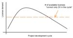
(6) “EDA licensing needs to adopt a SaaS model”
A very pointed argument by a DAC keynote speaker was that EDA licensing models are inconsistent with the trend to leverage cloud computing resources. He opined, “A stopped watch is correct twice a day – similarly, the amount of EDA licenses is right only twice in the overall schedule of a design project. The rest of the IT industry has embraced the Software as a Service model – EDA companies need to do the same.”
The figure below illustrates the “stopped watch licensing model”.
(The opportunity to periodically re-mix license quantities of specific EDA products in a multi-year license lease agreement mitigates the issue somewhat.) The keynote speaker acknowledged that changing the existing financial model for licensing would encounter considerable resistance from EDA companies.
(5) ML applications
There were numerous presentations on the growth anticipated for ML-specific designs, for both very high-end data center training/inference and for low-end/edge inference.
- high-end data center ML growth
For ML running in hyperscale data centers, the focus remains on improving the classification accuracy for image and natural language processing. One keynote speaker reminded the audience, “Although AI concepts are decades old, we’re really still in the very early stages of exploring ML architectures for these applications. The adaptation of GPGPU hardware to the ML computational workload really only began around 10 years ago. We’re constantly evolving to new network topologies, computational algorithms, and back-propagation training error optimization techniques.”
The figure below highlights the complexity of neural network growth for image classification over the past decade, showing the amount of computation required to improve classification accuracy.
(The left axis is the “Top 1” classification match accuracy to the labeled training dataset. One indication of the continued focus on improved accuracy is that neural networks used to be given credit for a classification match if the correct label was in the “Top 5” predictions.)
A considerable number of technical and trend presentations focused on adapting ML networks used for training to the stringent PPA and cost requirements of edge inference. High-precision data types for weights and intermediate network node results may be quantized to smaller, more-PPA efficient representations.
One presenter challenged the audience with the following scenario. “Consider Industrial IoT (IIoT) applications, where sensors and transducers integrated with low-cost microcontrollers provide real-time monitoring. In many cases, it’s not sufficient to simply detect a vibration or noise or pressure change or image defect that exceeds some threshold – it is necessary to classify the sensor output to a specific pattern and respond accordingly. This is ideally suited to the use of small ML engines running on a corresponding microcontroller. I bet many of you in the audience are already thinking of IIoT ML applications.”
(4) HLS and designer productivity
There were several presentations encouraging design teams to embrace higher levels of design abstraction, and correspondingly high-level synthesis, to address increasing SoC complexity.
Designers were encouraged to go to SystemC.org to learn of the latest progress in the definition of the SystemC language standard, and specifically, the SystemC synthesizable subset.
(3) clocks
Of all the challenges faced by design teams, it was clear from numerous DAC presentations that managing the growing number of clock domains in current SoC designs is paramount.
From an architectural perspective, setting up and (flawlessly) exercising clock domain crossing (CDC) checks for proper synchronization is crucial.
From a physical implementation perspective, developing clock cell placement and interconnect rouging strategies to achieve latency targets and observe skew constraints is exceedingly difficult. One insightful paper highlighted the challenges in (multiplexed) clock management and distribution for a PCIe5 IP macro.
Increasingly, physical synthesis flows are leveraging “useful skew” between clock arrival endpoints as another optimization method to address long path delays (and, as an indirect benefit, to distribute instantaneous switching activity). A compelling DAC paper highlighted how useful skew indeed helps close “late” timing, but may aggravate “early” timing paths, necessitating much greater delay buffering to fix hold paths. The author described a unique methodology to identify a combination of useful skew implementations to adjust both late and early clock arrival endpoints to reduce hold buffering, saving both power and block area.
Static timing analysis requires diligent attention to clock definitions and timing constraints – multiply that effort for multi-mode, multi-corner analysis across the range of operating conditions. One presentation focused on the need to focus on improved methods to characterize and analyze timing with statistical variation. In the future, it will become more common to tell project management that “the design is closed to n-sigma timing”.
(2) ML in EDA
There was lots of interest in how ML techniques are influencing EDA tools and flows. Here are some high-level observations:
One approach is to incorporate an ML technology directly within a tool algorithm. Here was a thought-provoking comment from a keynote talk: “The training of ML networks takes an input state, and forward calculates a result. There is an error function which serves as the optimization target. Back propagation of partial derivatives of this function with respect to existing network parameters drives the iterative training improvement. There are analogies in EDA – consider cell placement.”
The keynote speaker continued, “The current placement is used to calculate a result comprised of a combination of total net length estimates, local routing congestion, and critical net timing. The goal is to optimize this (weighted) result calculation. This is an ideal application to employ ML techniques within the cell placement optimization algorithm.”
Another methodology approach is to apply ML techniques “outside” an existing EDA tool/algorithm. For example, block physical implementation is an iterative process, from initial results using early RTL through subsequent RTL model releases. Additionally, physical engineers iterate on a single model using various combinations of constraints provided throughout the overall flow, to evaluate QoR differences. This accumulation of physical data over the development cycle can serve as the (design-specific) data set for ML training, helping the engineer develop an optimal flow.
(1) functional safety and security
Perhaps the most challenging, disruptive, and nonetheless exciting area impacting the entire design and EDA industry is the increasing requirement to address both functional safety and security requirements.
Although often mentioned together, functional safety and security are quite different, and according to one DAC presenter “may even conflict with each other”.
FuSa (for short) refers to the requisite hardware and software design features incorporated to respond to systematic and/or random failures. One presenter highlighted that the infrastructure is in place to enable designers to identify and trace the definition and validation of FuSa features, though the ISO 26262 and IEC 61508 standard structure, saying, “We know how to propagate FuSa data through flows and the supply chain. Correspondingly, we have confidence in the usage of software tools.” Yet, a member of the same panel said, “The challenge is now building the expertise to know where and how to insert FuSa features. How do you ensure the system will act appropriately when subjected to a random failure? We are still in the infancy of FuSa as an engineering discipline.”
The EDA industry has responded to the increasing importance of FuSA developments, by providing specific products to assist with ISO 26262 data dependency management and traceability.
Security issues have continued to arise throughout our industry. In short, security in electronic systems covers:
- side channel attacks (e.g., an adversary listening to emissions)
- malicious hardware (e.g., “Trojans” inserted in the manufacturing flow)
- reverse engineering (adversaries accessing design data)
- supply chain disruptions (e.g., clones, counterfeits, re-marked modules; the expectation is that die will be identified, authenticated, and tracked throughout)
The design implementation flow needs to add security hardware IP to protect against these attack “surfaces”.
Here’s a link to another SemiWiki article that covers in more detail the activities of the Accellera Security for Electronic Design Integration working group to help define security-related standards and establish a knowledge base of progress in addressing these issues – link.
To me, the impact of product FuSa and security requirements will have pervasive impacts on system design, IP development, and EDA tools/flows.
Can’t wait for the next DAC, on July 10-14, 2022, in San Francisco.
-chipguy