
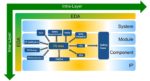
Functional safety has been at the forefront of the electrification of our vehicles with new ADAS features, and the push to reach autonomous driving, while having compliance with the ISO 26262 functional safety standard. I attended the Accellera hosted panel discussion on Monday at DAC, hearing from functional safety panelists that work at AMD, Arm, Texas Instruments, and DARPA. Alessandra Nardi, Accellera Functional Safety Working Group Chair moderated the panel discussion, and started out with a big picture overview first.
The Functional Safety Working Group (FS WG) started out as a proposed working group back in October 2019, and soon had a kickoff in December 2019. By February 2020 the working group was officially formed from member company representatives, and about 30 companies are now working on the standard. You can expect a Data Model definition white paper to come out in Q1 2022, and a Draft Language (LRM) release by Q2 2022.
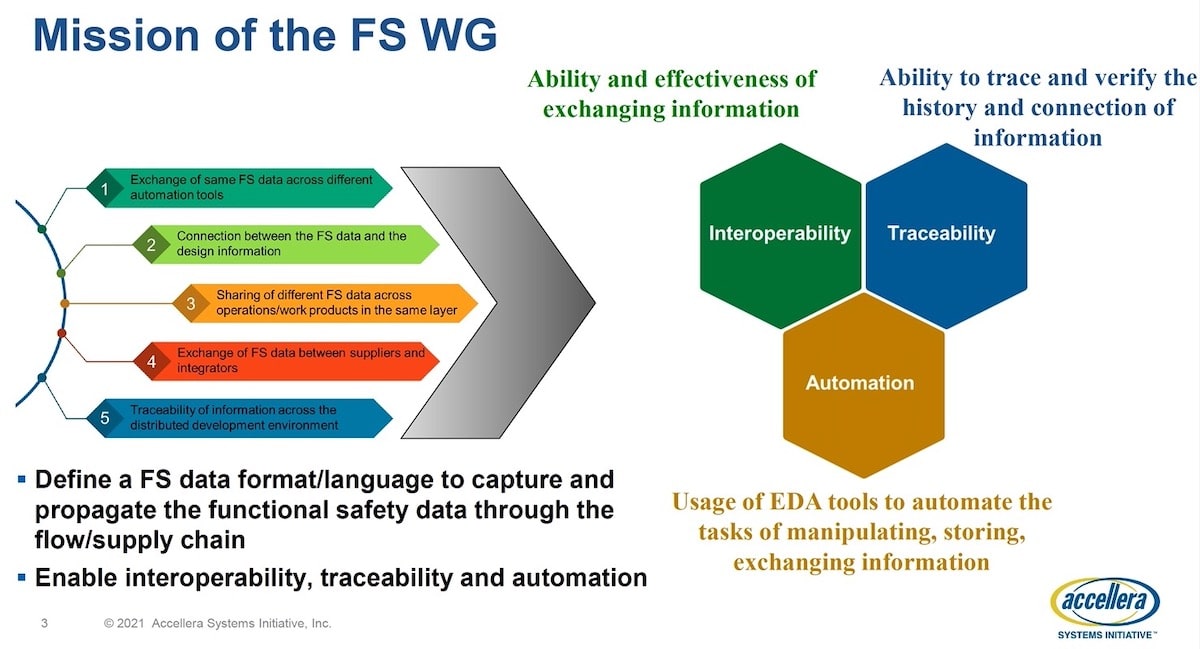
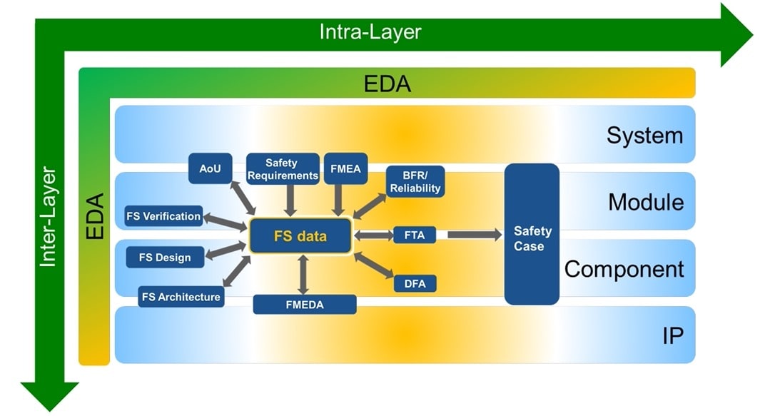
The big idea is to exchange the same FS data across different various automation tools, where there’s a connection between the FS data and the design info. So Accellera will define a data format/language.
Today there are many Functional Safety standards, like ISO 26262, and for industries like: Medical, Industrial, Aviation, Railways, Machinery. The Accellera FS WG will create a data standard, then collaborate with the IEEE as the standard becomes more mature, and they publish IEEE P2851.
AMD – Alexandre Palus
Functional Safety (FuSa) is concerned with both Systematic Failures and Random Failures. For vehicles, the Automotive Safety Integrity Level (ASIL) has defined four classes from A through D, where a failure in ASIL-D results in human death, and ASIL-B failures cause human injury.
Design for safety costs more on a project up front, but in the long run is less costly, based on experience, because there are fewer mask spins to correct safety issues. Teams really need to have a FuSa architect, and not treat FuSa as an after thought in order to be successful. If everyone does their job right, then nobody ends up in court.
Arm – Ghani Kanawati
Does FuSa add more complexity to development of a product? Yes, it’s a new requirement, but we need to convince design managers that FuSa is simple to implement. There may be conflicts during development between security and safety goals, and each project is unique in requirements, but safety concerns need to come into the project at the very beginning.
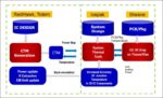
Having a lifecycle process in place ensures a higher chance of success when designing for FuSa. Here’s a typical lifecycle process for Soft IP development at Arm:
The FuSa design process does add more steps, and they are well understood, and sure, there’s a learning curve. If a random fault happens in your hardware design, then what happens to the system behavior? Does your system respond safely?
Texas Instruments – Bharat Rajaram
There are over a dozen FS standards spanning many inter-related industries, so ISO 26262 is the gold standard for semiconductor companies, and at TI they’ve been designing for safety since the 1980s. Automotive examples that require FuSa include:
- ASIL A – Rear lights, Vision ADAS
- ASIL B – Instrument cluster, headlights, rear-view cameras
- ASIL B&C – Active suspension
- ASIL C – Radar cruise control
- ASIL C&D – Engine management
- ASIL D – Antilock braking, electric power steering, airbag
Industrial systems have their own FuSa levels: SIL 1, SIL 2, SIL 3. Safety engineers are also concerned about Failure In Time (FIT) rates, where there are standards to follow like, IEC TR 62380, SN 29500, JESD85.
DARPA – Serge Leef
In Serge’s group they are mostly focused on security, not safety, but the two are related, because security breaches can cause safety failures. At DARPA one big concern is how to secure chips in the supply chain from gray market devices and hacking attempts. An electronic system has an attack surface reference model, and security exploits happen in four categories:
- Side Channel
- Reverse Engineering
- Supply Chain
- Malicious Hardware
The DARPA proposal is to harden new chips with an on-chip security engine:
Both Synopsys and Arm are working on the specification of this on-chip security engine, so stay tuned for more details.
Serge was skeptical of the FuSa concepts, based on experience working in EDA, because companies couldn’t explain clearly enough what compliance to the ISO 26262 standard meant for EDA tools that are used to develop IP. In government circles they talk about Quantifiable Assurance, which is FuSa for defense systems.
For most digital systems, with only 5-10% of the state space even being simulated, can you really assure that the chips will operate safely under all conditions?
Panel Discussion
Q: Are we going beyond 5% coverage of the digital state space?
A: Alessandra – optimistic about progress of continued FuSa best practices across many industries, and safety is becoming more mainstream now.
A: Alex – we started asking vendors back in 2002 and 2003 for FuSa, but they weren’t offering much. There’s been gradual improvements from Arm and EDA vendors, and we feel that cores are safe, and most IP is becoming safer. Most EDA and IP vendors have checkboxes for safety compliance. Yes, security is unsolved at the moment.
A: Bharat – Do you know how the aileron controller operate safely in a jet? They have 3 out of 5 microcontrollers vote. Even the S-Class Mercedes comes with about 200 controllers, and they have to meet FuSa standards to get into the car ecosystem. In the early days air gap approaches stopped hacking. By 2030 about 90% of cars will have connectivity, which also provides a huge attack surface for criminals.
A: Ghani – FuSa is really a tier of things to consider, while automotive vendors often are only willing to spend quite frugally. The ISO 26262 standard is about 300 pages in length now.
A: Serge – Hackers have breached cars with WiFi, and also through entertainment and CAN bus attacks, but where is the economic gain?
Q: How do you separate security from safety standards?
A; Ghani – yes, we’ve seen hacking in cars, so security and safety are always inter related.
A Alex – the security of SW in our cars is quite a recent development. Hackers could even place a Trojan into an auto company during development, and then trigger a ransom attack.
A: Serge – with the market push for autonomous vehicles, the security aspects are quite high.
Also Read:
Accellera Unveils PSS 2.0 – Production Ready


