

Tuesday at DAC was actually my very first time attending a technical session, and the presentation from Nebabie Kebebew, Siemens EDA, was called, Mitigating Variability Challenges of IPs for Robust Designs. There were three presentations scheduled for that particular Designer, IP and Embedded Systems track, but with the COVID precautions, only one presenter was on site. The technical paper authors were from both STMicroelectronics and Siemens EDA.
ST designs both digital and mixed-signal IPs for use in diverse applications like IoT, automotive and even AI, using process nodes from 90nm down to 18nm. For safety critical products like automotive chips, the challenge is to reduce the failure rate, measured in Parts Per Million (PPM). High-sigma verification is needed to meet the stringent PPM goals, and with each new process node the design sizes are getting more complex, causing even more simulation runs to verify across many Process, Voltage and Temperature (PVT) corners.
To reach the PPM goals would require high-sigma Monte Carlo circuit simulation for millions or billions of runs, something that is not feasible because the run times are just too long.
At ST they wanted to use one EDA tool flow to verify both standard cell libraries and memory IP across all PVT corners, using a smarter Monte Carlo simulation approach to achieve high-sigma verification in much less time.
Standard Cells
The challenge was that the standard cell libraries contained about 10,000 cells, and required 100 PVT corners to be simulated. Another factor was that IC design process variations are non-Gaussian at high-sigma.
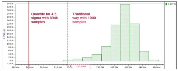
For example, the long-tail distribution of 894k samples on an internal node of a sequential cell is shown below:
The bars in Green are from running just 1,000 samples, and if we assumed a Gaussian distribution then linear extrapolation predicts a node value of 723mV at 4.5 Sigma. Using a worst-case of 894k samples, the actual worst node value is 680mV, which is about 50mV different versus linear extrapolation. For sequential cells like a Master Slave Flip-Flop you cannot use linear extrapolation to qualify high sigma, or wait long enough for brute force Monte Carlo results to complete.
An EDA tool from Siemens EDA called Solido Variation Designer addresses these exact issues with a two stage flow:
- Solido PVTMC Verifier
- Solido High-Sigma Tech
The first tool uses a machine learning algorithm to identify all of the worst-cast PVT corners, fast and accurate. Even the long-tail distributions are captured, and the approach dramatically reduces the actual number of PVT corners to be simulated.
The Solido High-Sigma Tech launches a SPICE simulator called Eldo to capture the rare simulation events at the highest-sigma points using only the worst-case PVT corners identified in the first tool, thus reducing the verification run times.
With this two stage flow to verify latch robustness at 6-sigma for a positive, edge-triggered Master Slave Flip-Flop, required only 20 PVT combinations:
- 5 process corners: FF, SS, FS, SF, TT
- 2 voltages: 0.80V +/- 10%
- 2 temperatures: -40C / 125C
Real SPICE circuit simulations were run at high-sigma conditions in order to capture the non-Gaussian long-tail behavior, but only on the worst PVT corners, resulting in high-sigma verification that was 10,000X faster than brute-force techniques.
Memory IP
Like with standard cells, there was a huge verification space for Memory IP with about 64 PVT combinations, and tens of IP instances. Netlists were quite large, with over 1M components. The bitcell on memory IP require a 6-sigma verification, and there are millions of bitcells on a memory IP block.
Using conventional verification methods an engineer would identify the memory instances with the smallest race margins and worst PVT corners, then run 300 Monte Carlo circuit simulations by sigma saturation on all of the race conditions, then assume a Gaussian distribution to determine the -5 sigma tail values. Drawbacks of this verification method are that you don’t know which PVT corners that race condition tail failures will occur, instances with larger nominal race margin values may have a larger sigma too, and the process deviates from Gaussian long-tail distributions.
Shown in red below are Gaussian approximations, while in reality the green curve shows actual variations.
Using the two stage flow with Solido Variation Designer on memory IP for 28nm and 40nm designs showed that high-sigma verification results could be obtained with 27,000 faster results, compared to brute-force Monte Carlo circuit simulations.
Summary
This group at ST has adopted a unified flow and methodology for standard cell libraries and memory IP verification, across PVT corners, while still modeling non-Gaussian behaviors, and achieving dramatic runtime reductions compared to brute-force Monte Carlo simulations, by using Solido Variation Designer. Nebabie also did a poster session on this paper at DAC.
Related Blogs
- Machine Learning Applied to IP Validation, Running on AWS Graviton2
- Siemens EDA Acquires an IP Validation Tool for standard cells, IO and Hard IP
- WEBINAR: Addressing Verification Challenges in the Development of Optimized SRAM Solutions with surecore and Mentor Solido
- Fast and Accurate Variation-Aware Mixed-Signal Verification of Time-Domain 2-Step ADC
- High Speed SerDes Design and Simulation Webinar Replay from Mentor


