The emergence of advanced packaging technologies has led to the introduction of new types of data communication interfaces. There are a number of topologies that are defined by the IEEE 802.3 standard, as well as the Optical Internetworking Common Electrical I/O CEI standard. [1,2] (Many of the configurations of interest involve connectivity between chips and electro-optical conversion modules for fiber communications.)
The figures below depict (some of) the classifications used to distinguish the physical characteristics of these interfaces.


The acronyms in the figures above are: Long Reach = LR; Medium Reach = MR; Very Short Reach = VSR; Extra Short-Reach = XSR; Ultra Short-Reach = USR.
For any interface, designers need to address the data throughput, power, area, and cost tradeoffs between implementations using parallel data bus and high-speed serial connections.
At the recent International Solid State Circuits Conference (ISSCC), researchers at Cadence presented their 7nm process node IP design solution for short-reach transceiver communications for die-to-die interfaces. [3] The remainder of this article summarizes the highlights of their presentation, and the unique features incorporated into their design.
Data Lanes, Data Rates, and Beachfront FOM
The SerDes differential signal pair topology is widely used for long-reach distances, but the additional embedded clock data recovery receiver overhead would be extremely inefficient for wide data interfaces at short distances.
For short-reach communications, specifically die-to-die interfaces on multi-die packages, parallel interfaces are used to provide the requisite composite data transfer rate. When designing the parallel interface, architects need to address the tradeoffs between the achievable transmitted data rate, signal losses at the receiver, routing resources required, and sources of (static) skew and (dynamic) jitter.
Specifically, individual pins/lanes in the parallel interface are grouped into a link, which includes data encoding — more on that shortly. A forwarded clock is sent with the data.

For the Cadence short-reach IP design, a link on the die consists of 7 Tx and 7 Rx data lanes, as illustrated in the top figure above. The bottom figure provides a Tx-to-Rx block diagram. The full IP macro is designed to support a 192-bit interface — the data is divided into 6 groups, 32 bits each. The Tx sends 6 bits of parallel data over the link, serialized over 32 cycles.
The metrics used to describe the implementation are:
- raw datarate per lane/pin
The Cadence short-reach IP provides 40Gb/sec/lane – more on how this is transmitted shortly.
- “beachfront”: expressed as effective datarate per mm, for the die edge
The Cadence short-reach IP provides 480Gb/sec/mm.
- power dissipation per bit: for example, 1.7pJ/bit
- signaling levels
The Cadence IP design chose single-ended, NRZ signaling; the transmitted signal level for successive ‘0’ and ‘1’ data values remains at the same voltage level. The implications of using a single-ended connection for the data, rather than a differential signal pair, were addressed using a clever data encoding method.
6/7b Data Encoding
In long-reach serial communications, there are numerous design issues to address, including:
- insertion and reflection losses, resulting in signal amplitude degradation
- (inductive) signal noise due to supply/GND switching current transients
- crosstalk between adjacent lanes
To address these issues, SerDes designers use:
- balanced routing, with focus on impedance matching for traces and vias
- differential signaling
- data encoding (e.g., 8/10b)
The first design criterion above focuses on improving the signal fidelity at the receiver. Differential signaling reduces the noise on the signals by balancing the supply/GND current distribution. To further enhance the current distribution temporal balance, eight bits of data are encoded into ten serially-transmitted bits, then decoded past the receiver. The encoding ensures an equal number of 1-to-0 and 0-to-1 transitions.
For the short-range parallel IP, Cadence designers also focused on defining:
- insertion loss/crosstalk ratio guidelines
- module trace layout and layer selection guidelines
- a 6/7b encoding for the parallel link
Like the 8/10b SerDes approach for (temporal) balance, the encoding of the data in each link improves the (spatial) balance in switching current transitions. The figure below illustrates the characteristics of the link encoding used.

The balance between transmitted ‘0’ and ‘1’ values in the parallel link 6/7b encoding provides “differential-like” switching, significantly reducing the magnitude of the ground current loops at both the Tx and Rx ends of the physical link.
Clock Generation and Data Calibration
A key feature of the Cadence IP is the generation of 40Gbps on a lane from the internal 10GHz PLL. Each data unit interval is one-fourth of the clock cycle. It is necessary to phase-align 4 separate clock taps derived from the 10GHz reference.

The Cadence design employs a unique strategy. The figure above illustrates how a set of pre-defined data patterns can be used to correct the duty cycle of each clock and the skew variation between clocks, each nominally shifted by one unit interval (90 degrees). For example, a repeating NRZ data transmit pattern of ‘….00110011….’ should align with the two edges of a clock. The transmit pattern ‘….00111100….’ should align across different clock edges. The most detailed transmit pattern of ‘….10101010….’ should align with the edges of successive clocks. For each of these patterns, the overall ratio of 1’s and 0’s is equal.

As depicted above, the transmit output is fed back into the Tx circuitry, and is sub-sampled at a lower frequency (the DIV clock generator in the figure). Each calibration step involves adjusting the duty cycle and clock phases until the sub-sampled output is 50%, for each pre-defined pattern. Seven unique data pattern calibration steps are applied, as illustrated below. The figure also illustrates the equivalent logic for transmitting the 40Gbps data.

For the Rx lane, the calibration steps are slightly more intricate, involving a sequence of communications with the Tx. The initial step adjusts the reference voltage to an input of the receiver data comparator, to align the switching threshold to the midpoint voltage of the transmitted data – a digital-to-analog converter (DAC) driven by the Rx controller establishes this voltage. The DAC output voltage to the comparator is dynamically adjusted during operation to maintain the (vertical eye center) voltage threshold over supply and temperature variations.
The second step is similar to the Tx clock phase alignment described above. The pre-defined set of Tx patterns for each lane captured at the receiver are used to adjust the phases of the Rx sampling clocks, derived from the forwarded clock in the link.
Testsite Results
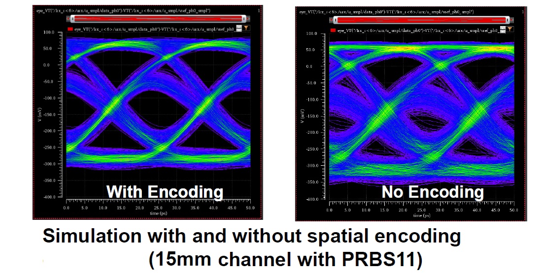
A micrograph of the IP testsite, the eye diagram, and the specs for the IP are shown in the figure below.


Note the improved eye diagram with the 6/7b spatial data encoding. The bit-error-rate (BER) curve is illustrated below.

Summary
The researchers at Cadence recently described their short-range transceiver design for the 7nm process node. The design includes several features of note:
- single-ended NRZ signaling
- a 6/7b data encoding scheme in the link, to minimize current switching noise
- a Tx/Rx clock phase alignment method using a set of pre-defined Tx data patterns
The resulting beachfront throughput and power efficiency are impressive. I would encourage you to peruse their ISSCC presentation.
Appendix
The emergence of advanced multi-die packaging – aka, “chiplet” packaging – has introduced a new class of high-speed (parallel) interface design, for SR/XSR/USR topologies. There has been quite a bit of industry commentary about the need for short-reach interface standards, to enable a broader adoption of chiplets from multiple sources. The Open Domain Specific Architecture (ODSA) consortium has taken on the challenge of driving standardization in this area. (link) The CHIPS Alliance has also been working on developing specifications for chiplet interfaces. (link)
Yet, as I was reading the Cadence ISSCC technical paper, it struck me that there are very unique features and a complex protocol for link training (with dynamic alignment over voltage and temp) that are a distinct differentiator. These features require a complete, full Tx-to-Rx end-to-end IP implementation between chiplets. The ODSA and CHIPS Alliance certainly have their work cut out for them, to enable Tx and Rx transceiver IP implementations from different sources. (The PCI-SIG has been able to climb this hurdle — it will be interesting to see how this evolves for chiplet interfaces.)
-chipguy
References
[1] https://www.ieee802.org/3/
[2] https://www.oiforum.com/technical-work/current-work/
[3] McCollough, K., et al., “A 480Gb/s/mm 1.7pJ/b Short-Reach Wireline Transceiver Using Single-Ended NRZ for Die-to-Die Applications”, ISSCC 2021, paper 11.3.
Also Read:
112G/56G SerDes – Select the Right PAM4 SerDes for Your Application
Lip-Bu Hyperscaler Cast Kicks off CadenceLIVE
How does TensorFlow Lite on Tensilica HiFi DSP IP Sound?
Share this post via:


Comments
There are no comments yet.
You must register or log in to view/post comments.