RVN! 26 Banner revised (800 x 100 px) (600 x 100 px)

SeaScape: EDA Platform for a Distributed Future

SeaScape: EDA Platform for a Distributed Future
by Daniel Nenni on 10-14-2021 at 6:00 am

EDA Platform for a Distributed Future

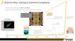
The electronic design community is well aware that it faces a daunting challenge to analyze and sign off the next generation of huge multi-die 3D-IC systems. Most of today’s EDA tools require extraordinary resources in specialized computers with terabytes of RAM and hundreds of processors. Customers don’t want to keep buying more of these expensive systems. It was interesting then to see an alternative approach discussed at the Ansys IDEAS Digital Forum that promises a more scalable approach to dealing with huge design sizes.

The session titled “SeaScape Analysis Platform – What’s Up and What’s Coming” was presented by Scott Johnson, senior engineer in the Ansys R&D team. Scott summed up the challenge as the need for a way to make use of the thousands of cheap, generic computers made available by commercial cloud providers. The proposed answer is called SeaScape and it shares many similarities with the open source Spark analytics engine from Apache. But SeaScape was created and designed specifically for EDA applications and it greatly simplifies the application of big-data techniques for electronic design. Users don’t need to worry about process messaging or resource scheduling or any of that. SeaScape’s internal scripting and user interface is based on Python – the world’s most popular coding language that comes with a huge open source ecosystem.

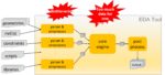
SeaScape is pre-built for the cloud and designed to require minimal setup. Scott stated that one of its primary benefits is the elastic compute resource allocation that allows every job to start as soon as even a single CPU is ready, and more CPUs will be conscripted as they become available and as required by the tool.

Instant start-up and easy cloud deployment are just two of the major benefits offered by SeaScape’s big-data distributed data processing technology

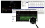
Following this introduction to SeaScape Scott turned his focus to practical deployment of SeaScape.  The first product implementation was in Ansys RedHawk-SC. RedHawk is the EDA industry golden signoff tool for chip power integrity analysis. RedHawk has been ported onto the SeaScape data platform and is now RedHawk-SC, which is currently in widespread production use at most leading semiconductor houses.

One of the really unique features over traditional EDA tools made possible in RedHawk-SC thanks to SeaScape is that a single session can simultaneously analyze multiple views, scenarios, and PVT corners. That means that a single RedHawk-SC session will generate multiple extraction views in the physical space, multiple transient analyses, multiple signal integrity views, and so forth.

The consequence of this massive parallelism is that additional analytics become possible that were never available before. This includes predictive analytics derived when things like switching activity, physical location, and timing criticality are combined in true multi-variable analysis to create an avoidance score that tells designers early on what things probably will work well and what won’t. As Scott points out, “Having this breadth of data available at your fingertips is a game changer!”. Customers can also customize RedHawk-SC’s analyses and tailor them to their signoff needs through the Python scripting interface.

SeaScape is in production use in RedHawk-SC for power integrity signoff of some of the world’s largest digital chips. It’s ability to analyze multiple operational corners at the same time is a huge advance in speed and analytics

The last section of Scott’s presentation described some of the advanced capabilities on offer in RedHawk-SC that were made possible by SeaScape. These include:

  • Reliable analysis of dynamic voltage drop (DvD) by simultaneously analyzing many thousands of possible switching scenarios in order to give extremely high coverage.
  • DvD diagnosis capabilities that untangle which cells are the ultimate root causes of observed voltage drops and focus debugging effort in the right places.
  • Use the analysis data to perform very fast ‘what-if’ queries in a matter of seconds
  • Construct hierarchical reduced order models (ROM) that capture the essentials of the interactions between multiple components with much faster runtimes
  • Analyze the low-frequency power noise in the package so their impact can be decoupled from the analysis of high-frequency power noise in each chip. This speeds up analysis where both slow and fast signals interact

Scott summarized SeaScape as a better way forward to handle today’s huge design sizes and rising complexity by harnessing the power of many small machines in the cloud, completing even the biggest tasks in a single day, and bringing together disparate data sources to improve the quality and power of information delivered to the user.

More technical sessions and designer case studies are available at Ansys IDEAS Digital forum at www.ansys.com/ideas .

Also Read

Ansys Talks About HFSS EM Solver Breakthroughs

Ansys IDEAS Digital Forum 2021 Offers an Expanded Scope on the Future of Electronic Design

Have STA and SPICE Run Out of Steam for Clock Analysis?


Webinar – SoC Planning for a Modern, Component-Based Approach

Webinar – SoC Planning for a Modern, Component-Based Approach
by Mike Gianfagna on 10-13-2021 at 10:00 am

Webinar – SoC Planning for a Modern Component Based Approach

We all know that project planning and tracking are critical for any complex undertaking, especially a complex SoC design project. We also know that IP management is critical for these same kinds of projects – there is lots of IP from many sources being integrated in any SoC these days. If you don’t keep track of what you’re using and how it’s used there will be chaos. What isn’t discussed as much is how these two disciplines interact – what are the benefits of a holistic approach? This was the focus of a recent webinar from Perforce. The synergies and benefits of a comprehensive approach are substantial. Read on to learn about SoC planning for a modern, component-based approach.

Johan Karlsson

First up is Johan Karlsson, senior consultant and Agile expert at Perforce. Johan elaborates on planning strategies that are useful for SoC design. He points out that SoC projects are becoming more software-centric, and this creates opportunities. Johan reviews the various strategies available for planning complex projects.

He begins with a discussion of the traditional “deadline tracking” type of approach. The mindset here incudes:

  • Visualizing fixed deadlines and what leads up to them
  • Handling hard dependencies between different work activities
  • Rolling wave planning details

Managing the dependencies and the impact of changes is key for this approach. Approaches for implementation include:

  • Work breakdown structure
  • Gannt scheduling

Another approach Johan discusses is something called the lean approach. This technique focuses on delivering customer value in a just-in-time way. Quality is key here, with lots of root cause analysis to find and improve process steps. The customer, in this context could be the end customer or an internal team that is involved in the project. The approach focuses on flow and looks for areas where waste can be reduced.  The principles here include:

  • Value: satisfy customer needs just in time
  • Flow: locating waste generated by the way a process is organized
  • Quality: is built-in

Approaches for implementation can include:

  • Whiteboard
  • Post-it notes of different colors
  • Pens

The final approach is adaptive techniques. Here, an agile approach is taken. The methodology is very similar to what is used in software development – it can be applied to management of IC design as well. The driving philosophy of this approach is the Agile Manifesto, summarized as follows:

  • Individuals and interactions over process and tools
  • Working software (or hardware) over comprehensive documentation
  • Customer collaboration over contract negotiation
  • Responding to change over following the plan

A SCRUM framework can be used for implementation:

  • Roles (product owner, SCRUM master)
  • Events/meetings (sprint planning, daily stand-ups, sprint reviews)
  • Artifacts (product backlog, sprint backlog, etc.)

Johan then discusses the reality of real projects, where a hybrid, or mixed-use approach of all three methods will typically work best. There are excellent insights offered here about what will work best in real projects and how various approaches can be implemented. I highly recommend you get these insights directly from Johan. I webinar replay link is coming. Spoiler alert: Hansoft from Perforce provides an excellent backbone to implement a customized, targeted planning approach.

Simon Butler

The next presenter is Simon Butler, general manager, Methodics IPLM. IP Lifecycle Management (IPLM) has been covered quite a bit by SemiWiki. You can get a good overview of IPLM here. Simon begins with a good overview of the fundamentals of IPLM. It’s worth repeating here:

  • The fundamental use model in IPLM is hierarchical configuration management of the project IP (component) list
    • Some of these IPs will be outsourced or off the shelf, others internally developed
    • IPLM enables a robust release flow managing internal and external component versions
  • The IPLM release flow can be integrated directly into your verification flow and enforce quality control on your release candidates
    • Releases of the required quality can be automatically inserted into the overall hierarchy, with versioning to ensure traceability

Simon goes on to explain the various parts of the design that can be tracked – both the data and metadata. A great explanation of how to implement these concepts in a design flow is also presented, complete with a discussion of the bill of materials and how it is managed. A methodology to unify the management and tracking of IP and its impact on the overall project plan is presented by Simon, along with an example.

At this point, I started to see the benefits of unifying these two disciplines. IP effects the design project and vice versa. Keeping track of all of it in one unified environment is quite appealing. During the webinar, a convenient Semiconductor Starter Pack is offered. This package contains all the tools needed to implement a complete IC and IP tracking/management flow. This is a great way to experience the benefits of a unified approach. If some of the items discussed seem relevant to your design projects, you can check out the webinar here. It also includes a very relevant Q&A section.  Now you can find out about SoC planning for a modern, component-based approach.

Also Read

You Get What You Measure – How to Design Impossible SoCs with Perforce

Achieving Scalability Means No More Silos

Future of Semiconductor Design: 2022 Predictions and Trends


TSMC Arizona Fab Cost Revisited

TSMC Arizona Fab Cost Revisited
by Scotten Jones on 10-13-2021 at 8:00 am

TSMC North America Fabs

Back in May of 2020 I published some comparisons of the cost to run a TSMC fab in Arizona versus their fabs in Taiwan. I found the fab operating cost based on the country-to-country difference to only be 3.4% higher in the US and then I found an additional 3.8% because of the smaller fab scale. Since that time, I have continued to encounter reports that the US fab costs are approximately 30% higher than countries in Asia. In the studies I have found, most of the cost difference is attributed to “incentives” without a clear explanation of what the incentives are. My calculation does not include incentives but still the size of the difference led me to completely reexamine my assumptions and look into incentives, what they could be and how they would impact the costs I calculate.

Profit and Loss

At the highest-level companies are judged by their Profit and Loss (P&L) and I decided to go through a simple P&L line by line and look at every country-to-country difference that could impact the bottom line profitability.

A P&L is summarized on an income statement, a simple income statement is:

  1. Revenue – the money received from selling the product
  2. Cost of Goods Sold (COGS) – the direct costs to produce the product being sold. This is what our Models calculate.
  3. Gross Margin = Revenue – COGS. For wafer sale prices we estimate gross margin and apply it to the wafer cost.
  4. Period expenses – Research and Development expenses (R&D), Selling, General and Administration expenses (SG&A) and other expenses.
  5. Operating Income = Gross Margin – Period Expenses
  6. Income Before Tax = Operating Income – Interest and Other
  7. Net Income = Income Before Tax – Tax (tax is based on Income Before Tax)

We can then go through this line by line to look at country by country differences. These line numbers will be referenced below in bold/italics.

For a cost evaluation line 1. Is irrelevant.

Line 2. (COGS) Is a key differentiator.

Cost of Goods Sold

In our Models we break out wafer cost categories as follows:

  • Starting Wafer
  • Direct labor
  • Depreciation
  • Equipment Maintenance
  • Indirect Labor
  • Facilities
  • Consumables

Starting wafers – our belief is that starting wafers are globally sourced and the country where they are purchased does not impact the price. This has been confirmed in multiple expert interviews including by wafer suppliers.

Direct Labor (DL) – all our Models have DL rates by country and year for 24 countries. In 2021 the difference in labor rate from the least expensive to most expensive country was 21x! For each wafer size and product type we have estimates of labor hours required and we calculate the direct labor cost. We believe this calculation accurately reflect cost differences between countries in all our Models. It should be noted here, that leading edge 300mm wafer fabs are so highly automated that there are very few labor hours in the process and even with a huge labor rate difference, the percentage impact on wafer cost is small.

Depreciation – this is the most complex category. The capital cost to build a wafer fab is depreciated over time to yield with the depreciation amount charged off to the P&L.

We break out the capital cost to build a facility into:

  1. Equipment – we believe equipment is globally sourced and the cost is basically the same in any country. We did get one input that the US cost are slightly higher due to import costs, but we don’t believe this is significant.
  2. Equipment Installation – install costs in our Models are based on equipment type with different costs assigned to; inspection and metrology equipment, lithography equipment, and other equipment types (ALD, CVD, PVD, etc.). What we have found in our interviews is the costs vary by country with the variation being different for the different categories. For example, inspection and metrology equipment installation is heavily weighted toward electrical work that varies in cost between countries. Other equipment is more heavily weighted toward process hookups that are less country dependent. Lithography equipment is intermediate between the two.
  3. Automation – we believe automation is globally sourced and does not change in cost between countries although we are still checking on this assumption.
  4. Building – in the past we assumed that building costs were the same by country believing the major components were globally sourced. In our expert interviews we found there is a significant difference in cost per country. Revisiting fab construction costs we have in our databases also found differences after accounting for product types. Our latest Strategic Cost and Price Model fully accounts for these differences.
  5. Building Systems – as with the building we assumed building systems were globally sourced and the cost didn’t vary by country, but this only partially true. Our latest Strategic Cost and Price Model fully accounts for these differences.
  6. Capital Incentives – if a company receives government grants to help pay for the investments to build a wafer fab, they will impact the actual capital outlay for the company building the Fab. In the past we have not accounted for this, we now allow capital incentives to be entered into the model.

Our models all calculate the capital investment by fab using a detailed bottoms-up calculation. The equipment, equipment installs, and automation are then depreciated over five years, the building systems over ten years and the building over fifteen years. We use these default values because most companies use these lifetimes for reporting purpose. There are lifetimes by country differences for tax purposes, but taxes and reporting values are typically calculated separately. There are some companies that don’t use five years for equipment but to enable consistent comparison between fabs we use five years as a default, although the ability to change the lifetimes is built into many of our Models.

Equipment Maintenance – equipment maintenance costs include consumable items, repair parts and service contracts. The technicians and engineers that maintain equipment at a company are accounted for in the Indirect Labor Cost described below.

In our Strategic Cost and Price Model the country differences are accounted for as follows:

  1. Consumables – we continue to believe this is the same by country but there are company to company differences. For example, an etcher has quartz rings in the etch chamber that some companies source from the Original Equipment Manufacturers and other companies may source in the secondary market at lower cost.
  2. Repair Parts – repair parts are distinct from consumables in that they aren’t expected to normally wear out during operation. We believe these are globally sourced and don’t vary in cost by country.
  3. Service Contracts – we believe there is some difference in service contract costs due to labor rate differences.

Our latest Strategic Cost and Price Model fully accounts for these differences.

Indirect Labor (IDL) – IDL is made up of engineers, technicians, supervisors and managers, our Models have engineer salaries by country for twenty-four countries by year and ratios are used to calculate the technician, supervisor, and manager salaries. Difference in engineer salaries vary by 12x between the lowest cost and highest cost countries. For each process/fab being modeled we look at the IDL hours required for the process and break out the IDL hours between the four IDL categories. We believe all our Models correctly reflect country to country differences currently. As with DL costs, IDL costs have less impact on wafer cost than you might expect but are more significant than DL costs.

Facilities – we break out facilities into Ultrapure Water, Water and Sewer, Electric, Natural Gas, Communications, Building Systems Maintenance, Facility Occupancy, and Insurance. The main costs are Electric, Natural Gas, Building Systems Maintenance, and Insurance. Our Models all account for Electric and natural gas rates by country for twenty-four countries. Electrical rates vary by 2.8x by country and natural gas by 7.6x by country and both are fully accounted for in the models. Facility system maintenance and facility occupancy also vary by country. Our latest Strategic Cost and Price Model fully accounts for these differences.

Consumables – all our Models calculate consumables in varying degrees of detail. We believe materials are sourced globally and do not vary in price by country. There are some country-to-country tariff differences but the implementation of this is so complex and constantly changing that we do not model. It. We do not believe the impact is significant.

Profit and Loss – Continued

 Line 3 – Gross Margin

Gross Margin isn’t part of a COGS discussion but many of our customers buy wafers from foundries. Foundry wafer prices are Wafer Cost + Foundry Margin and we have put significant effort into providing Foundry Margin guidance in our models. Foundry Margins in our Models vary company to company and within a company by year and quarter, purchasing volume and process node. They are not country dependent.

Line 4 – Period Expenses

 Not relevant to a wafer cost discussion

Line 5 Operating Income

Not relevant to a wafer cost discussion

There are two other places in the P&L where we may see country-to-country impact.

Line 6 Income Before Taxes

if a government offers a company low-cost loan this would reduce interest expenses in the interest line. In my opinion low-cost loans are incentives.

Line 7 Net Income

Tax – there are two pieces to the tax line, one is country-to-country tax rate differences and the other is preferential tax rates. In my opinion tax rate differences are a structural difference whereas a preferential tax rate is an incentive. For example, the corporate tax rate in the US is 25.8% and in Taiwan is 20%. These tax rates are normally applied to Income Before Taxes.

In summary we see country to country operating cost differences and our current release of our Strategic Cost and Price Model models these differences accurately and in detail.

There is also country to country tax rate differences that we don’t model because they are below the COGS line.

Finally, there are incentives, we see these as having three parts:

  1. Capital grants that would reduce capital cost and therefore depreciation in COGS.
  2. Low-rate loans that would impact interest expenses.
  3. Tax incentives, investment, R&D and other tax reductions.

TSMC Arizona Fab

Having reviewed all the elements of wafer cost difference we can now investigate how TSMC’s cost in Arizona will match up to their cost in Taiwan.

TSMC currently produces 5nm wafers in Fab 18 – phases 1, 2, and 3 in Taiwan. We believe each phase is current running 40,000 wafer per month (wpm) with plans to ramp to 80,000 wpm per phase over the next two years. In contrast the Arizona fab is planned to produce 20,000 wpm (at least initially). This will lead to three differences in costs:

  1. Country to country operating cost difference – after accounting for all the operating cost differences, we now find a 7% increase in cost to operate in Arizona versus Taiwan. We find a higher difference than we did previously due to now including some factors we had previously missed. Having reviewed a P&L line by line and consulting with a wide range of experts we do not believe there are any missing parts to this analysis. An interesting note here is direct labor cost in the US are over 3x the rate in Taiwan, but they have only minimal impact because in Taiwan direct labor is only 0.1% of the wafer cost and even tripling or quadrupling the labor rate it is still less than 1% of the wafer cost. Utility costs are the other hand are lower in the US.
  2. Fab size differences – accounting for a 20,000 wpm fab in the US versus 80,000 wpm in Taiwan, plus the efficiency of clustering multiple fabs together in Taiwan adds 10% to the country-to-country difference found in 1. For a total 17% difference. We want to highlight that the 10% additional cost is due to TSMC’s decision to build a small fab in the US. We expect the initial Arizona cleanroom to have room to ramp up to more than 20,000 wpm and the site to have room for additional cleanrooms. Over time if TSMC ramps up and expands the site the 10% difference can be reduced or eliminated.
  3. Incentives – to the best of my knowledge Taiwan does not offer direct capital grants. To the best of my knowledge Taiwan does not offer low-cost loans. In the past Taiwan offered tax rebates for capital investment in fabs but my understand is this program has ended. There are R&D tax rebates available, and Taiwan has a lower corporate tax rate than the US (although this isn’t an “incentive” in my view). To investigate the tax advantage for TSMC in Taiwan versus the US I have compared TSMC’s effective tax rate over the last three years to Intel’s effective tax rate in the last three years. Surprisingly they aren’t that different, now I know there is a lot of complex financial engineering in Taxes, but it is the best comparison I can find. TSMC ‘s tax rate for 2018, 2019 and 2020 is 11.7%, 11.4% and 11.4% respectively. Over the same period Intel’s tax rate was 9.7% (one-time benefits) in 2018, 12.5%, in 2019, and 16.7% (NAND Sale) in 2020. So over three years TSMC paid 11.5% and Intel paid 13.1% as a tax rate which isn’t that different.

Conclusion

The bottom line to all this is the cost for TSMC to make wafers in the US is only 7% higher than Taiwan if they built the same size fab complex in the US as what they have in Taiwan. Because they are building a smaller Fab complex the cost will be 17% higher but that is due to TSMC’s decision to build a smaller fab, at least initially.

I do want to point out this doesn’t mean the US is not at a bigger cost disadvantage versus any other country. India has reportedly discussed providing 50% of the cost of a fab as part of an attempt to get Taiwanese companies to set up a fab in India. At least in the past the national and regional governments in China have offered large incentives. Israel has also provided significant incentives to Intel in the past. But under current conditions a US fab is only 7% more expensive than a fab in Taiwan if all factors other than the location are the same.

Also Read:

Intel Accelerated

VLSI Technology Symposium – Imec Alternate 3D NAND Word Line Materials

VLSI Technology Symposium – Imec Forksheet


AI and ML for Sanity Regressions

AI and ML for Sanity Regressions
by Bernard Murphy on 10-13-2021 at 6:00 am

machine learning for regressions min

You probably know the value proposition for using AI and ML (machine learning) in simulation regressions. There are lots of knobs you can tweak on a simulator, all there to help you squeeze more seconds, or minutes out of a run. If you know how to use those options. But often it’s easier to talk to your friendly AE, get a reasonable default setup and stick with that. Consider that a sort of one-step learning.

However, what works well in one case may not be optimal in others. Learning must evolve as designs and test cases change. You can’t reasonably call the AE in for every run, and you shouldn’t have to. ML can automate the learning. Which makes sense, but what I had not realized is that one of the big impact areas for this technology is for sanity regressions. Vishwanath (Vish) Gunge of Microsoft elaborated at Synopsys Verification Day 2021.

Why short regressions are such a good fit

Sanity tests are those tests you run to make sure you (or someone else) didn’t do something stupid. Like accidentally checking in code that you hadn’t finished fixing. Or leaving a high verbosity debug switched turned on. When you want to integrate all the code in a big subsystem of the whole SoC, probabilities of a basic mistake add up quickly. We design sanity tests to smoke these problems out quickly. Because the last thing you want is to launch overnight regressions, then come back in the morning to garbage results. Sanity tests are designed to run quickly, maybe a few minutes, at most say 30 minutes, in parallel across many machines.

Seems like that wouldn’t be where you would find a big win in ML optimization. But you’d be wrong. It’s not the test run-time that matters, it’s the frequency of those tests. Vish said that in their environment, sanity regressions consume huge compute resources, running many times per day. Which I read as them using those regressions in the best possible way – flushing out basic mistakes as a per-designer level, a per-subsystem level and a full integration level. When a mistake is found, a sanity test (or tests) must be re-run. Lot of checking before time is invested in expensive full regressions. Which is why ML can have an important impact.

VCS DPO

Synopsys VCS® offers a dynamic performance optimization (DPO) option based on both proprietary and ML methods. I don’t know the internal details, but it is interesting that they use other methods in addition to ML. ML is the hot topic these days but it’s not always the most efficient way to get to a good result. Rule-based systems can be more semantically aware and converge quicker to an approximate solution, from which ML can then further optimize. At least that’s my guess.

That said, this is AI/ML so there is a “training” phase and an “application” phase. All packaged for ease of use, no AI skills required by the end user.

Dynamic performance optimization in action

Vish presented analysis comparing the non-AI (base-level) run-time with learning phase and the application phase on the same set of sanity runs. For DPO they used all optimization apps available as a starting point, for example FGP (fine-grained parallelism) with multiple cores. Naturally learning phase runs were slower than the base level, perhaps by ~30%. However, application runs were on average 25% faster, allowing them to do ~30% more of these regressions per day.

Vish stressed that some thought is required to get maximum benefit in these flows since learning takes more time than base runs. He suggested running learning once every few days as the design is evolving, to keep optimizations reasonably current as design and tests change. Learning can run less frequently as the project is nearing signoff since optimum settings shouldn’t be expected to change as often.

A very interesting and practical review. You can learn more from the recorded session. Vish’s talk is one of the early sessions on Day 2.

Also Read:

IBM and HPE Keynotes at Synopsys Verification Day

Reliability Analysis for Mission-Critical IC design

Why Optimizing 3DIC Designs Calls for a New Approach


Ansys Talks About HFSS EM Solver Breakthroughs

Ansys Talks About HFSS EM Solver Breakthroughs
by Tom Simon on 10-12-2021 at 10:00 am

HFSS scaling over the years

Ansys HFSS™ has long enjoyed industry respect as a highly accurate electromagnetic simulator suitable for general purpose applications. Ansys has worked over the years to maintain its gold reference accuracy, and also to dramatically improve its performance and ease of use. A very interesting review of the key technology breakthroughs over the years is covered in an on-demand presentation by Jim Delap, Director of Product Management at Ansys. The presentation, part of the Ansys IDEAS Digital Forum event, titled “Breakthroughs in Electromagnetic Simulation” covers HFSS from the very early days in the 1990’s up to the present. In the last decade in particular there have been major strides in addressing designs that would have been unthinkable just a few years ago.

To set the stage Jim begins by reviewing the performance and capacity of HFSS when it was released in 1990 as the world’s first commercial electromagnetic simulation product. At the time they illustrated its use on a coax-waveguide transition that needed a ~10k element matrix to solve. A single frequency run required 16 hours. Today this same design can be run in about 20 seconds on a laptop!

At the heart of HFSS’s reliability and accuracy is the automatic adaptive meshing, which increases the efficiency of the simulations by only placing mesh elements where they are needed. Once design setup is completed by defining geometry, materials, boundaries, excitations and solve setup, HFSS automatically goes through the solution process which includes: initial mesh, adaptive refinements, frequency sweep and final post processing steps.

Analyzing production tool usage, Ansys found the matrix solver is where most of the time is spent. So according to Jim this is where they have focused much of their development effort. Initially they implemented Matrix Multiprocessing to take advantage of multiprocessor machines. Now they have advanced versions of this that use techniques that work on sparse matrices. In real world cases they can achieve a 5X improvement in runtime with 10 cores. Not content to limit users to the processors on a single machine, Ansys has also developed a Distributed Memory Matrix solver that allows runs to access more memory and more cores. Jim talks about an example where they model a car trunk antenna with a simulation volume that includes the entire vehicle and surrounding area. The matrix size was 12M elements, using 715GB of memory and 6 machines. The runtime in 2016 was 3 hours. The runtime would be significantly reduced today. Currently they can solve models with over 100M unknowns, which means that full RFIC chips can be fully modeled for EM coupling in under a day.

To improve the runtime of frequency sweeps, HFSS introduced Spectral Decomposition Method (SDM) that solves frequency points in parallel for a 1.7X speed-up on the same hardware. Using additional high-performance compute clusters dramatically improved runtime by over 5X so that runs that used to require over a day can be done in a matter of hours. Then the next step was the introduction of S-Parameter Only Matrix Solve which further improved frequency sweep runtime by significantly reducing memory consumption. The on-demand presentation video goes into the specific benefits from these improvements.

More recently Ansys has focused on advances in meshing to independently mesh separate regions of the design using different algorithms. For instance, objects have widely different scales, i.e. chips, boards, connectors, antennas, are each meshed separately and in parallel. The separately meshed objects are then combined into a single solution volume. These enhancements allow for solving a wide range of systems from chips, boards, full products, all the way up to test chambers in a single simulation.

Ansys also has a new Phi Plus mesher that can handle bond wires, packages and ECAD/MCAD assemblies. Jim says that it is the first real conformal mesher. Using 12 cores it offers a 10.7X speed up. It is ideally suited for bond wires and other irregular structures. The improved meshes it creates enable much faster convergence resulting in faster sweep times. In some of their test cases Jim says the new Phi Plus mesher is nearly 18X faster than the classic mesher.

HFSS scaling over the years

The combination of Mesh Fusion and Phi Plus Mesher is, according to Jim: “The one-two punch for meshing. We are now meshing and solving problems that we never thought were meshable”.

The final part of the presentation moves away from speed and focusses instead on technologies that are aimed at increasing the size of problems that HFSS can take on. Jim talks about HFSS’s Domain Decomposition method (DDM) that works as a distributed memory solver that can parse out subdomains to distributed processors. Jim emphasizes that it is a true solver not simply separate S-Parameter generation with stitching of results. The mesh domains are automatically generated, making the entire process much easier for users.

Jim also touches on several topics at the end of his talk including improvements for finite antenna arrays and faster broadband adaptive meshing. He also discusses the running of HFSS on Ansys Cloud hosted on Miscrosoft Azure and supported through the Ansys Engineering Desktop (AEDT). It has been quite an evolution from running a single coax-waveguide transition to the ability to model a full chip, on a board, in a finished product (such as a car) including the measurement chamber. The presentation goes into sufficient detail to make a convincing case that Ansys has and will continue to innovate HFSS to meet the most complex electromagnetic simulation challenges. While the market offerings for EM solvers has increased and the number of companies offering them has grown, it is clear that HFSS still stands in a class of its own. The full presentation can be viewed on demand as part of the Ansys IDEAS Digital Forum at www.ansys.com/ideas.

Also Read

Ansys IDEAS Digital Forum 2021 Offers an Expanded Scope on the Future of Electronic Design

Have STA and SPICE Run Out of Steam for Clock Analysis?

Extreme Optics Innovation with Ansys SPEOS, Powered by NVIDIA GPUs


ESD Alliance Reports Double-Digit Growth – The Hits Just Keep Coming

ESD Alliance Reports Double-Digit Growth – The Hits Just Keep Coming
by Mike Gianfagna on 10-12-2021 at 6:00 am

ESD Alliance Reports Double Digit Growth – The Hits Just Keep Coming

The latest Electronic Design Market Data report was just published. The headline announces continued substantial growth for the sector: Electronic System Design Industry Logs Double-Digit Q2 2021 Year-Over-Year Revenue Growth, ESD Alliance Reports. While not quite the record-breaking growth reported last quarter, the news is extremely upbeat. We should be careful about getting complacent about EDA and IP growth as these segments are influenced by a lot of factors that tend to be cyclical, and at times highly variable and unpredictable. Let’s look at the data to try and understand why the hits just keep coming.

The Numbers

As reported in the press release, “Electronic System Design (ESD) industry revenue increased 14.6% year-over-year from $2,783.9 million to $3,191.4 million in Q2 2021.” First, let’s examine revenue by product and application and the year-over-year change:

  • CAE revenue increased 10.1% to $1,014.6 million. The four-quarter CAE moving average increased 11%.
  • IC Physical Design and Verification revenue decreased 0.4% to $581.5 million. The four-quarter moving average for the category rose 18.6%.
  • Printed Circuit Board and Multi-Chip Module (PCB and MCM) revenue increased 16.8% to $284.4 million. The four-quarter moving average for PCB and MCM increased 9.4%.
  • SIP revenue rose 27.1% to $1,204.9 million. The four-quarter SIP moving average grew 20.5%.
  • Services revenue increased 23.1% to $106.1 million. The four-quarter Services moving average increased 8.8%.

IC physical design and verification stands out with a decrease. Dan and I spent some time chatting with Wally Rhines, Executive Sponsor, SEMI Electronic Design Market Data report. Wally pointed out that physical verification is a bit “lumpy” in terms of consumption. There are huge demands on this technology near tapeout. Wally also pointed out that the overall four quarter trend is quite healthy. If you’re looking for bad news, you will likely not find it here.

 Looking at the same trends on a regional basis, we see:

  • The Americas, the largest reporting region by revenue, purchased $1,367.3 million of electronic system design products and services in Q2 2021, an 18.3% increase. The four-quarter moving average for the Americas rose 15.2%.
  • Europe, Middle East, and Africa revenue increased 9.9% to $415 million. The four-quarter moving average for EMEA grew 7.8%.
  • Japan revenue decreased 1% to $237.9 million. The four-quarter moving average for Japan rose 1.9%.
  • Asia Pacific revenue increased 15.9% to $1,171.2 million. The four-quarter moving average for APAC increased 22.9%.

As always, the numbers tell one story. By spending time with Wally, we got some of the backstory as well.

The Narrative

Wally’s comments in the press release include, “Product categories Computer Aided Engineering (CAE), Printed Circuit Board and Multi-Chip Module (PCB and MCM), Semiconductor IP (SIP), and Services all reported double-digit growth. Geographically, all regions reported growth on a rolling four-quarter basis, with the Americas; Asia Pacific (APAC); and Europe, Middle East, and Africa (EMEA) showing a substantial year-over-year increase.”

Wally opened our conversation with more direct comments, “We hit another big one. 14.6 percent. The onslaught of demand continues.” Wally also pointed out that “PCB is back”, with higher growth numbers this quarter. We talked a bit about China. The consumption of EDA and IP is strong there. A growing percentage of that consumption is to fuel domestic demand vs. export. There is a question around how large the domestic EDA and IP segment can become in China, which could shift revenue from the US for example.

At present, it appears the growth of these industries is slow in China. We all know EDA is difficult, and so is building domestic core infrastructure and technology. That said, there is a growing number of EDA companies in China so that is worth watching. We touched on a lot of topics in search of a material downward trend and found none. As we said goodbye, I kept thinking, the hits just keep coming. You can learn more about ESD Design Alliance Electronic Design Market Data here

Also read:

Is EDA Growth Unstoppable?

The Juggernaut Continues as ESD Alliance Reports Record Revenue Growth for Q4 2020

ESD Alliance Report for Q3 2020 Presents an Upbeat Snapshot That is Up and to the Right


High Reliability Power Management Chip Simulation and Verification for Automotive Electronics

High Reliability Power Management Chip Simulation and Verification for Automotive Electronics
by Daniel Payne on 10-11-2021 at 10:00 am

iWave waveform min

Automotive electronics bring strong demand for power management chips, but its strict reliability requirements also pose new challenges for chip designers. The chip needs to be able to work in various harsh environments such as high temperature, low temperature, aging, abnormal power supply, etc. Although the traditional measurement-based method is effective, it has high cost and low efficiency. Multi-scenario high-precision simulation and verification is an inevitable choice that can not only meet the requirements of the testability standards of automotive chips, but also improve design efficiency at a lower cost. For comprehensive functional verification, it will need thousands or even tens of thousands of simulations. The power-on process of some power management chips can be very slow, which can be as high as 80% of the total time.

The discontinuity of the high-voltage device model in the power management chip often leads to non-convergence of the simulation. Engineers need to constantly adjust the option combination to make the simulator converge. However, they often encounter situations where they are exhausted and can only rely on the manufacturer’s technical support.

In terms of reliability of a working chip, power-on is not enough to meet the design requirement. We usually need to monitor the complete working process of the chip. For example, when the chip is working, the voltage and current overload or high impedance state of the node will cause unpredictable risks to the chip. The current solution in the industry is to provide a circuit check function. But the drawback of this scheme is that the designer cannot efficiently locate the real problem of the design based on circuit check’s result. The reason is that existing solutions will output a large amount of text data, and designers need to extract effective information from the massive data. Even if the problem of a certain node is found, it is difficult to combine this problem with the circuit.

Corner Switch Technology to accelerate simulation and verification

Empyrean Technology’s analog circuit design environment platform can provide an efficient multi-corner simulation configuration environment through the corner center. Through Corner Switch Technology, it can better deal with convergence problems caused by model and circuit parameter jumps. Using this technology, the chip designer can cut off the simulation, replace the corner, or change the model and circuit parameters after the circuit simulation is powered on, and quickly perform simulation analysis on the power-on state under different PVT conditions. Because the power-on process has little difference under different corner conditions, therefore, we can use normal corner for initial simulation. The state after power-on needs to be closely monitored. Therefore, the more simulation jobs you have, the more you will save in the total simulation time with the help of Corner Switch Technology.

Circuit Diagnoser to check circuit status

Empyrean Technology’s analog circuit design platform provides  Circuit Diagnoser platform, which can summarize the circuit abnormalities during circuit simulation and display them in an orderly manner. For example, at time A, the gate and source of device M5 have voltage overload; at time B, the current of net8 exceeds the threshold for metal current density. When one wants to find the device M5 or net8 in the circuit, the designer only needs to click the corresponding abnormal result in the Circuit Diagnoser to back-annotate the device and node in the schematic. Combined with Empyrean Technology’s MDE platform and iWave waveform display tool, the designer can perform synchronous functional analysis on the abnormal results, waveforms, and schematic structures of the problem nodes.

Summary

Automotive electronics is the market with the highest requirements for chip reliability, and power management chips occupy the highest proportion of analog chips. Empyrean Technology’s high-reliability power management chip simulation and verification solution has been verified in the automotive electronics industry. Designers of other types of analog chips with high reliability requirements can also benefit from Corner Switch and Circuit Diagnoser solutions to accelerate the comprehensive simulation and verification of circuit functions.

Related Blogs


Hardware Data Acceleration for Semiconductor Design

Hardware Data Acceleration for Semiconductor Design
by Kalar Rajendiran on 10-11-2021 at 6:00 am

What if you could Table

This blog is a follow-on piece to an earlier one titled NetApp’s ONTAP Enables Engineering Productivity Boost.  If you have not had an opportunity to read that blog,  please do so for context. Using real life examples, it showcases how customers could improve real-world design engineering productivity as much as 10%.

For the engineers within all of us, this blog will begin by explaining how the Snapshots and FlexClone features of ONTAP system work.  It will then describe where you can immediately deploy this into your design flow for productivity boosts. Although EDA design flow is used for illustration purposes, this works well for software development workflows too.

As a rehash of the first blog, the premises was the following.

What If you could…

How would you reimagine your EDA and SW development workflows if your design DATA were Agile?

What Makes Instant Data Copies Possible?

NetApp’s ONTAP storage operating system has two key data acceleration features you could build into your design flow with simple RESTful API calls.

  • Snapshots, which makes “Instant volume level READ-ONLY back-ups or copy” possible
  • FlexClone, which makes “Instant volume level READ/WRITEABLE copy” possible

The ONTAP storage operating system takes simple API calls and operates on massive data sets without the data leaving the storage controller.  The concept is similar to how graphics accelerators work. They take simple API calls from the CPU and manipulate gigantic numbers of pixels in the video framebuffer to create complex video images.

Snapshots can be derived from existing volumes of data to create Read-only copies. The snapshot names are specified through the respective API calls. The Figure below shows an active volume of data (Vol1) where each of block A, B, C, and D represents a file (or logical block of data).  When a snapshot is created, the physical blocks of data are not copied, only the pointers to the data are copied.  This makes instant data copies possible.  An added value of this approach is the storage efficiency gained, as the data itself is not copied.

FlexClones can be derived from existing volumes of data to create fully READ/WRITEABLE copies.  Clones are created just as snapshots are, by copying just the pointers to the data. Clones provide the same added value of storage efficiency as snapshots do. A clone takes up incremental storage only when modifications are made to the data.

That is “Data Accelerated”

Snapshots and clones are very fast and very storage efficient. The API calls make it very easy to create them and the operating system makes it very easy to use.  And it typically takes seconds to either snapshot or clone 1GB, 1TB or 1PB of design data. To an application, both snapshots and clones look and behave just like a normal storage volume.

Using Snapshots and FlexClones in Your Design Flow

Let’s look at where and how in your design flow you can benefit by using snapshots and flexclones. We will divide the design phase into development, tapeout and post-tapeout ECO.

During Development Phase

Most chip design flows use modern Continuous Integration (CI) build processes. Design commits (code check-in) go through a CI smoke test verification process before the file is “integrated” into the branch or mainline code.  Integrated code is run through larger Nightly build and test suite to further verify code integrity and quality.  Then Release builds create Release Candidate builds until a final build meets all the feature quality goals and is ready for tapeout.

  • Fast workspace creation

Engineers spend a considerable amount of time checking files out of source control tools like SOS or Perforce and then building views of the chip.  As designs get bigger, the time taken to checkout and build a development workspace grows. To speed up this process, teams try different implementations.

NetApp’s ONTAP storage system allows you to snapshot each CI, Nightly and Release candidate build volume with a label. Dev and verification engineers can then create flexclones of the latest “Good” CI or Nightly build.  Within seconds, they would have a personal copy of the source code for that build including all the build artifacts from that build.  Build artifacts might include simulation views, synthesis .db/.gate files, log files, etc.

Hours of checkout and build time can be reduced to minutes.

  • Faster bug fixes and design closure

If a bug is found in a CI, Nightly or Release candidate build, there is a lot of time overhead in both setting up the workspace before debugging and in committing the change.

Using ONTAP’s FlexClone function, an engineer can instantly create a clone of the failing CI, Nightly or Release candidate build for use in their debugging effort. Time taken to reproducing the bug, fixing it and achieving design closure is accelerated.  This results in better utilization and efficiency of two of the most expensive resources (engineers and EDA licenses).

  • Faster Continuous Integration (CI Builds)

Modern DevOps processes ensure design integrity by checking each and every design commit as soon as the code is committed. The processes do not wait until a Nightly build to test build quality.  These modern DevOps practices have dramatically reduced the time to detect build errors and rework time.  During busy commit periods right before a milestone build, critical changes can get stuck in a log jam of CI builds.

DevOps teams have tried to accelerate the CI process by various means such as building parallel CI build pipelines, checking out multiple baseline code directories and applying and testing multiple code commits in parallel.

ONTAP data acceleration can improve modern DevOps process flows.

Refer to the Figure below.

A FlexClone can be created from the snapshot of the last known good build, new code can then be integrated and retested. When a new baseline CI build is established, a new snapshot can be created, and the process repeated.  This approach parallelizes the CI process and eliminates bottlenecks while shortening the time for code integration and retesting.

With API driven snapshot names, you can quickly and easily create checkpoints and restore points for your project throughout the development phase.  This allows for increased innovation as engineers can freely try bold changes without worrying about main database corruption.

Tapeout

At the end of the development phase, the entire database is massive in size. It includes everything from the RTL stage to GDSII. It is standard practice to make a golden copy of this entire database at the time of backend release (tapeout). But how to ensure that the golden copy stays golden? How to prevent inadvertent modifications of files inside the final project directory?

Simply add an API call to your design flow to create a volume level snapshot with a name that speaks for itself. Example names for this snapshot could be “ProjA_final_v20210922” or “ProjA_tapeout_<build_id>”, where the build_id relates back to an ICManage/P4 integration ID.

During Post-Tapeout ECO Phase

What about an ECO modification post tapeout?  When a post-tapeout ECO needs to happen, engineers are under more intense time pressure. You want to speed up the ECO fix/test cycle with the ability to easily rollback if a mistake creeped in during the bug fix.

Simply make a clone of the golden copy snapshot made at the time of tapeout. If the ECO is to fix a bug, you may decide to assign parallel teams to speed up the process. As the clones consume disk space only for modifications, you can create multiple clones, one for each team. Each team can test their changes in their own clone copy. Once tested, the changes can be merged back into the original volume.

When the ECO is released, simply apply a new snapshot name such as “ProjA_final_v20210922_ECO_A” that is self-descriptive.  Now you have a golden copy of the ECO version and the original golden copy is still intact.

As you can see, use of snapshots and clones in an ECO flow can dramatically speedup iterations and enable rapid and easy rollbacks if and when needed.

Ready to transform your engineering environment?

If you are already using NetApp for your chip or software development, you already have what you need to get started. If you’re already familiar with how to make ONTAP system’s API calls, you can immediately start benefitting by implementing as described above. Otherwise, stay tuned for the next blog in this series.

The next blog will delve into the technical details of NetApp’s Open Source DataOps Toolkit. Gaining familiarity with this toolkit will shorten the learning curve for implementing Snapshots and FlexClones in your Design flow.

If you’re not currently using NetApp, you may want to seriously explore leveraging it, going forward.


IAA Mobility: The Un-Car Show

IAA Mobility: The Un-Car Show
by Roger C. Lanctot on 10-10-2021 at 6:00 am

IAA Mobility The Un Car Show

IAA Mobility held in Munich last month was the first post-pandemic international auto show to take place outside of China. The organizers positioned automotive displays in city-center plazas while car companies rubbed shoulders with large suppliers and tiny startups on the show floor at the conference center.

Attendees would have been forgiven for confusing IAA with Hannover’s CeBIT of old or even Las Vegas’ CES, though it was not nearly as large as either of those events.  IAA Mobility brought a unique un-car show vibe to the world of car shows with two halls devoted to bicycles and e-bikes, a large outdoor test drive area, and multiple stages for speakers to expound on sustainability and electrification.

Attendance was robust, though figures were not available. There were some notable non-exhibitors including Toyota, Nissan, Honda, Stellantis, and Volvo, among others.  Participants were nearly universally masked and international travelers could obtain free COVID-19 tests on-site for their return flights.

The two most important announcements at the event included Mobileye’s planned launch of a robotaxi service in Munich in cooperation with leading global rental car company Sixt creating – with Moovit – two multimodal transportation platforms; and Renault’s Megane E-Tech, an EV crossover equipped with 26 safety features and running Google’s Android operating system and cloud services from its 24-inch screen on Qualcomm’s Snapdragon processor – the beginning of a tidal wave of Qualcomm/Google-equipped cars to come in 2022.

Most notable of all, though, with the onset of 5G poised to alter the automotive industry, was the absence of wireless carriers at the show. This absence was striking given the fact that BMW brought its iX Vision car to IAA Mobility. Set for early 2022 availability, the iX EV crossover is likely to be the first 5G-equipped car available to consumers outside of China.

The iX will be equipped with a first-of-its-kind dual SIM solution enabling owners to add their car to an existing wireless plan for a one-time 10 Euro activation fee. After that initial fee, a Vodafone “One Number Car” plan will cost €5 a month.

BMW is also bringing 5G to the i4 and the so-called “Personal eSIM” functions enabled by BMW and Vodafone will be portable. Customers will be able to transfer the settings of the Personal eSIM to other 5G-enabled BMWs including rental or loaned vehicles.

Nevertheless, neither Vodafone, Deutsche Telekom, nor Orange saw fit to present their connectivity products, services, or vision for the emerging world of multi-modal mobility at IAA.  Google and Apple were two other notable no-shows, though both companies run their own events for users and partners.

Google, with a main office near the Marienplatz in downtown Munich, provided panel moderators and speakers to the robust agenda of presentations on a wide range of transportation and technology topics.  You could smell the existential anxiety in the air at IAA with car makers shifting their powertrains to electricity while experts continued to debate the merits of hydrogen propulsion.

The importance of 5G connectivity appeared to get short shrift. Wireless marketing messages related to connecting cars was left to Qualcomm and Huawei.  In fact, much of the entire car connectivity ecosystem was not present at IAA Mobility – the chipset and module makers, eSIM suppliers, connectivity platform operators, and such.

This disconnect from the connectivity community was notable as many of the safety systems and fleet operations described by robotaxi operators, Tier 1 suppliers, and the car makers at IAA Mobility themselves rely on connectivity. Even car radios – notably that latest Mercedes EQ line-up – leverage connectivity for metadata and to integrate with streaming sources.

Car makers have a common cause with carriers in “selling” 5G connectivity in cars to consumers. Strategy Analytics surveys show a growing interest in connectivity among car buyers, but the competition with smartphone use in cars remains problematic.  Car makers are making an increasingly strong case for consumers to pay for telematics services – tying advanced safety features such as GM’s Super Cruise to these services – but consumers continue to opt out.

Connected cars with no connections will increasingly become a problem for car makers dependent on leveraging over-the-air software updates to keep systems up to date.  Even essential map updates and mandated requirements – such as Intelligent Speed Assistant set for a 2024 EU implementation – require connections.

Wireless carriers themselves still find it difficult to prioritize vehicle connectivity with billions in revenue flowing from smartphones and enterprise applications. The low prioritization assigned to connecting cars is especially odd given the EU mandate for eCall connectivity devices in cars.

IAA was only the latest reminder that car connectivity appears to be an afterthought for carriers – in the context of auto show participation. The un-car nature of IAA Mobility might produce a rethink next time around.

The reality is that wireless carriers around the world are actively engaged with the auto industry as 5G networks are deployed and edge computing technology is put to work to test and deploy smart city solutions integrating cars into the wireless grid.  Perhaps carriers can be forgiven for overlooking IAA in its inaugural year.  Carriers are usually absent from auto shows after all.

IAA Mobility was exceptional.  It was a car show that was something more. A different story of transportation’s future was being told at IAA Mobility.  It was certainly car-centric – but it marked a shift toward a more integrated mobility solutions event filled with startups and other application developers along with auto makers and leading industry suppliers.  It’s a different kind of show for a different kind of market and a different kind of mindset.


Podcast EP42: Semiconductor Materials Innovations

Podcast EP42: Semiconductor Materials Innovations
by Daniel Nenni on 10-08-2021 at 10:00 am

Dan is joined by Alex Yoon, head of strategic and emerging technologies at Intermolecular. Dan and Alex explore the application of Intermolecular’s materials research capabilities, including their prototype fab in the Bay Area.

https://intermolecular.com/

The views, thoughts, and opinions expressed in these podcasts belong solely to the speaker, and not to the speaker’s employer, organization, committee or any other group or individual.