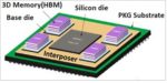
ads mdx semiwiki building trust gen 800x100ai

Optical I/O Solutions for Next-Generation Computing Systems

Optical I/O Solutions for Next-Generation Computing Systems
by Tom Simon on 10-28-2021 at 10:00 am

Multiphysics design

According to DARPA the fraction of total power consumed in semiconductors for I/O purposes as been growing rapidly and is creating an I/O power bottleneck. It has reached the point where it needs to be addressed with new technologies and approaches. Interestingly, while the energy density, as measured by pJ/bit for short reach IO – such as chip to chip in the same system – is low, there are so many more connections and higher data volumes that the overall energy required is often higher than in rack to rack connections. Dries Vercruysse, Senior Photonics Design Engineer at Ayer Labs, recently gave a talk at the Ansys Ideas Digital Forum 2021 on how they were motivated to use optical technology for chip to chip communication. He pointed out that the energy efficiency density of longer reach connections has long benefited from the use of optical technology.

There are many hurdles to taking photonics methods for board to board and scaling them so they are effective and efficient enough for use between individual packages. Dries describes how Ayer Labs has developed a solution based on optical modulation using micro-ring resonators.  They have created tunable voltage-controlled resonators that are 1000x smaller than optical devices in traditional ethernet transceivers and are compatible with 300nm CMOS technology. An off-chip laser is coupled from fiber to chip via a vertical grating coupler and then amplitude modulated by varying the bias voltage across the resonator.

Because resonators that operate at different wavelengths can be created by varying physical parameters, one fiber can support many signals in parallel via wavelength division multiplexing (WDM). A single off-chip laser can provide the light source needed for many chips. The Ayer Labs chiplet contains multiple drivers and receivers that then interface externally through short fiber connections to other chips and can be tightly integrated with FPGAs via in-package system-on-chip (SoC).

Dries talked about a Link Demo they performed that connected two chips that each used the Ayer Labs TeraPHY CMOS Optical IO chip. With a remote light source and a bi-directional link, they achieved energy use of <5pJ/bit for both 16Gbps and 25Gbps. The fiber operated at ~5.3 microwatt average power/lambda. During the demo they transferred 104.165 terabits of data without any errors.

Multiphysics Design

Creating this system required extensive simulation of the electrical, physical and optical performance characteristics in their TeraPHY chiplet. For instance, the resonator has semiconductor junctions, optical paths, and even a small thermal heater to help rigidly control the thermal environment. According to Dries this was a perfect example of Multiphysics design. Time frames for each domain were orders of magnitudes apart as well. From picoseconds for the optical, to microseconds for the thermal. They used a wide range of Ansys tools to facilitate their development. The waveguide alone required GPU accelerated IOSMF FDTD simulations with over 1.6 trillion grid points. This was accomplished using the cloud compute environment offered by Ansys.

Ayer labs has already had design success and notable design wins leading to integrations into advanced SoC packages. Dries highlighted their work with Intel FPGAs, including a design that is on a standard PCIe card. Previously, the use of optical fiber was a pipe dream for chip to chip communications. Ayer has shown that it is not only feasible, but it can be effective. The key to their development was having the ability to fully model Multiphysics behavior in a complex environment. The full presentation from the Ansys Ideas Digital Forum 2021 is available for viewing here.

Also Read

Neural Network Growth Requires Unprecedented Semiconductor Scaling

SeaScape: EDA Platform for a Distributed Future

Ansys Talks About HFSS EM Solver Breakthroughs


Memory Consistency Checks at RTL. Innovation in Verification

Memory Consistency Checks at RTL. Innovation in Verification
by Bernard Murphy on 10-28-2021 at 6:00 am

Innovation New

Multicore systems working with shared memory must support a well-defined model for consistency of thread accesses to that memory. There are multiple possible consistency models. Can a design team run memory consistency checks at RTL? Paul Cunningham (GM, Verification at Cadence), Raúl Camposano (Silicon Catalyst, entrepreneur, former Synopsys CTO) and I continue our series on research ideas. As always, feedback welcome.

The Innovation

This month’s pick is RTLCheck: Verifying the Memory Consistency of RTL Designs. The paper was published in the 2017 IEEE/ACM MICRO. The authors are from Princeton and NVIDIA.

Memory consistency is a contract between hardware and software developers on ordering of reads and writes in a multicore system. If two or more threads can load from or store to a logical memory location, given no necessary synchronization between cores and optimizations like out-of-order execution, some orders may be allowed and some may not. There are multiple possible ways to define such rules. An agreed set of rules bounding this behavior defines a memory consistency model (MCM). RTLCheck is the authors’ contribution to automatically check that an RTL design complies with a set of (modified) user-defined axioms encoding an MCM.

The method detects axiom violations as cycles in “happens before” (hb) graphs of test cases, elaborated as fetch-decode/execute-writeback operations across cores. One such litmus test checks message passing between cores. Since arcs in an hb graph denote permitted orderings of operations, a cycle in an hb graph implies a sequence of operations that must complete before they start, which is not possible. The axioms used to prove to an MCM work with abstract architecture specifications. Temporal proof engines used in formal methods for RTL lack this flexibility (per the authors) so axioms are “synthesized” to industry standard System Verilog Assertions (SVA) and constraints with some limitations on what can be mapped.

Paul’s view

Verifying memory consistency in multi-processor (MP) systems is hard, and I’m always a fan of raising abstraction levels as a important way to tackle hard verification problems. The paper’s basic premise to compile high level micro-architecture MCM axioms into SVA is a great idea, and the “happens before” graphs used in these axioms are an elegant and intuitive way to express MCM intent.

The paper is thorough and it’s always nice to see joint research between academia and industry. The authors clearly describe their approach and provide a full worked example on an open-source RISC-V core in which they found a real bug using their methods. Although, as the authors point out, the bug is a bug even for a single instance of the RISC-V core. The memory’s “ready” signal has been accidentally tied to high so the memory is always ready to accept a new value.

I do find myself wondering how much simpler the author’s axiomatic specifications in “Check” tool format are than their synthesized industry standard SVA equivalents. The mapping is 1-1, just more verbose in SVA format. For example, one key observation in the paper is that an SVA for “A implies B happens later” (A |-> ##[1:$] B) can match the case where A happens multiple times before B where an hb-graph axiomatic equivalent would not – imagine that A is “store value x” and B is “load value x”. An intervening “store value y” would obviously invalidate the axiom. Synthesizing additional SVA syntax to prevent multiple A’s before B is one of the paper’s contributions (A |-> ##[0:$]!A ##1 B), but this contribution feels more like syntactic sugaring than a fundamental raising of the abstraction level.

Overall, tight paper, well written, and on an important topic. Also, nice to see the author’s using Cadence’s Jasper formal tool to prove their synthesized SVAs. And find that RISC-V bug 😃

Raúl’s view

For the interested reader, the paper explains axiomatic microarchitectural models in 𝜇spec (first-order logic). Together with the corresponding 𝜇hb (happens-before) graphs and temporal assertions. They walk through a small motivating example with two cores . Each runs a small common “message passing” litmus test of 2 instructions in each core which is easy to follow. The actual generation of the temporal assertions is quite complex and involves additional user non-automatic steps:

  • mapping the litmus test program instructions and values to RTL expressions
  • mapping 𝜇hb graph nodes to Verilog expressions

This requires a “user” with deep knowledge of the field, i.e. axiomatic specifications, 𝜇spec, SVA, RTL, etc. Designers of parallel architectures working with verification experts and access to JasperGold and the check suite [33] can potentially profit from using RTLCheck.

The results are nice: For a 4-core RISC-V, 89% of the generated assertions for 56 litmus tests are completely proven. The remaining 11% complete with bounded proofs. These include the discovery of a real bug in the Multi-V processor and its fix.

As an academic research paper, I find the claims and results stand up, and the concept to be very interesting. However, it is hard to see commercial opportunity in productizing this work. The very high and necessary level of cross-domain expertise and what appears to be a significant level of manual effort does not seem scalable to production applications.

My view

I had hoped this would be a neat lateral way to verify coherency. But Paul and Raúl talked me out of it. The expertise and effort required to setup axioms and constraints to manage formal analysis on a modern SoC seems daunting. I hold out hope that the core concept may still have value. Perhaps when applied (in some manner) in a simulation application.

Also Read

Cadence Reveals Front-to-Back Safety

An ISA-like Accelerator Abstraction. Innovation in Verification

Accelerating Exhaustive and Complete Verification of RISC-V Processors


Intel- Analysts/Investor flub shows disconnect on Intel, Industry & challenges

Intel- Analysts/Investor flub shows disconnect on Intel, Industry & challenges
by Robert Maire on 10-27-2021 at 2:00 pm

Pat Gelsinger Triple Spend

Analysts missed all warning signs until Intel spelled it out
12% stock drop shows disconnect and misunderstanding
No quick fix, this is a long term, uncertain problem & solution
Everyone ignored the obvious until it ran them over

A 12% stock drop is fault of investors/analysts not Intel

Whenever a stock drops 12% in one day there is some sort of major disconnect between the company and the street. Sometimes companies keep bad news under wraps until the quarterly call or just don’t do a good job of “managing expectations” on the street. Sometimes analysts miss not too subtle hints and information until the company spells it out directly.

In the case of Intel’s recent stock drop it is more the fault of analysts and investors missing the obvious rather than the company not communicating. Its also “analysts” not doing some very simple analysis…

Its all about lower margins-more expenses or less revenue or both

It seems that the street completely missed how bad margins would get and for how long. None of this should have been such a surprise as we know Intel’s expenses have and will be going up and that revenues are under pressure from competition and shortages. So it must be the magnitude of those issues that is a surprise

A perfect storm of triple and quadruple spending

We coined a phrase earlier this year about Intel having to “triple spend” that means; 1) spend a lot of money to catch up to TSMC and their technological lead 2) Spend money and margin to have TSMC (their enemy) supply chips for Intel to sell because Intel is lacking in technology and/or capacity 3) Spend money to try to become a foundry player.

We later amended our “triple spend” scenario to “quadruple spend” to account for the spend to acquire GloFo or something like it. Any one of these spend items represents a huge sum of money but taken together it represents a tidal wave of a hemorrhage of money that can hobble even Intel.

More importantly, all four of these new spending sprees is not a one and done, one time spend but rather a long term multi year commitment for each effort.

Missing simple math

Even though the numbers are readily available it seems relatively few people, if anyone, bothered to add and look at the potential sum of spend and the impact it would have on Intel’s expense structure.

Analysts should have able to figure out that capex wasn’t just going to go up 20% year on year and be enough to catch TSMC spending $25B a year, twice Intel. Its clear that Intel has to spend TSMC-like sums of CAPEX and then some more in order to catch TSMC. If we use EUV tool count as a proxy for spend ( which is a good approximation) they need to outspend TSMC now to make up for years of under investment and under buying.

TSMC does not work for free and will not give away its precious leading edge capacity to a company that wants to beat it, without extracting a pound of flesh. TSMC has Intel in a tough position and will squeeze for what its worth and Intel has no choice but to pay up otherwise TSMC will turn on the AMD floodgates.

Becoming a foundry player is not just the $20B to build two fabs in Arizona(let alone fabs in Europe…) and fill them with equipment. Its hiring lots of people (let alone finding the talent) and building the infrastructure (or buying it) needed to service silicon customers. Something Intel wasn’t able to accomplish in the past. Building the two fabs and all associated foundry expenses for something that may not show revenue for years and take a long time to ramp will be a huge drain.

In the meantime renewed competition from AMD (whose product is being built in the same TSMC fabs as Intel) and others as well as emerging competition (like Apple, ARM, Google, Facebook etc…) will negatively impact revenues and pricing. Bottom line is Intel is caught in a longer term margin squeeze.

We were very clear about this and warned investors long ago, before anyone

Way back on March 23rd of this year when Intel announced its foundry intentions we wrote;

Either Intel will have to start printing money or profits will suffer near term

We have been saying that Intel is going to be in a tight financial squeeze as they were going to have reduced gross margins by increasing outsourcing to TSMC while at the same time re-building their manufacturing…essentially having a period of almost double costs (or at least very elevated costs).

The problem just got even worse as Intel is now stuck with “triple spending”. Spending (or gross margins loss) on TSMC, re-building their own fabs and now a third cost of building additional foundry capacity for outside customers.
We don’t see how Intel avoids a financial hit.

Link to original “Foundry Fantasy” note

I don’t think I could have been any clearer, but obviously the message was not received.

Back on January 21st, 10 months ago we said:

Get ready for numbers to look ugly and get sandbagged

Although Intel did not give full years guidance, we would hold onto our seats as we have suggested that the dual costs of increased outsourcing to TSMC added to increased spend on Internal efforts to regain Moore’s Law pace will be high and pressure margins in the short term which we would view as at least the next two years and maybe more.

If Pat is smart he will sandbag strongly and lower expectations to numbers that can be beaten easily and overestimate the costs of fixing 7NM and ramping capacity while still paying TSMC to make chips. He doesn’t want to put out numbers he will miss in his first couple of quarters on the job.

We would hope that this would include a large jump in Capex and R&D to give the engineers and manufacturing the latitude they need.

We were right about the numbers getting ugly but obviously Intel did not “sandbag” enough or manage street expectations enough.

The bottom line is that this margin issue has all been a very long time in the making and should not have been a surprise that cratered the stock. It was all out in the open. If I could figure it out then all the well paid analysts at the large investment banks should have figured it out as well.

Obviously that was not the case as there was a spate of analyst downgrades and shock and surprise that sent the stock tumbling.

The relationship between success and money spent is non linear

One would think that with all the talk about the amount of money (margin) that Intel will be spending that success will be a virtual “lock”. That is far from the case and not reality.

You can throw a lot of money at Moore’s law and still have no guarantee of success. Likewise the foundry business is not a “If we build it, they will come” field of dreams.

Even with all the financial hardship and margin pressure success is not pre-ordained.

This means that we would take statements like all the sacrifice now will be worth it for the future success, with a grain of salt. There is still very high risk in execution as the tasks at hand are huge and complex and its not simply a matter of throwing money at it….but it helps a lot.

The stocks

Even with the 12% drop there is still a lot of risk and a lot of financial pain ahead and we maintain our view that Intel’s stock is better off viewed from the side line. We could see a dead cat bounce or those who feel that there’s a price opportunity but we still see risk and issues for the investable future.

Obviously the semiconductor equipment companies will benefit from increased Intel spend but we already assumed that. Some companies such as ASML will see modest positive impact as they are sold out for 18 months so it matters little to them.

We view the stock action as more of a reality reset rather than any sort of true fundamental change as nothing really changed investors just finally got the memo.

For all those “analysts” who missed the memo we can offer a discount on our newsletter.

Also Read:

LRCX- Good Results Despite Supply Chain “Headwinds”- Is Memory Market OK?

ASML- Speed Limits in an Overheated Market- Supply Chain Kinks- Long Term Intact

Its all about the Transistors- 57 Billion reasons why Apple/TSMC are crushing it


Webinar: A Practical Approach to FinFET Layout Automation That Really Works

Webinar: A Practical Approach to FinFET Layout Automation That Really Works
by Mike Gianfagna on 10-27-2021 at 10:00 am

Webina A Practical Approach to FinFET Layout Automation That Really Works

There are certain tasks that have been the holy grail of EDA for some time. A real silicon compiler – high level language as input and an optimal, correct layout as output is one. Fully automated analog design – objectives as input, optimal circuit as output is another. With the increased layout times, due to the ever-increasing design requirements at advanced process nodes, the automation of advanced node custom layout – high-level commands that implement complex layout tasks with one click, has become another of these holy grails. While I don’t think we’ll see a viable approach for the first two any time soon, I’m here to tell you the third item is indeed available today. Read on to learn about a practical approach to FinFET layout automation that really works.

Background

Pengwei Qian

Dan Nenni was recently joined by Pengwei Qian, the founder and CEO of SkillCAD. You can learn more about Pengwei and his remarkable company in this interview. What followed was a compelling discussion about a new tool from SkillCAD that does address one of the holy grail items, above. There was also a detailed demo to prove it works. The entire event is captured in a webinar. A replay link is coming. First, a bit about SkillCAD, the new product and what you will see in the demo.

SkillCAD was founded in 2007 to enhance the productivity of Cadence Virtuoso by providing capabilities not offered by the Virtuoso environment. Today, over 85 companies use SkillCAD. The webinar details a new product from SkillCAD – IC Layout Automation Suite (LAS) Advanced. This product is focused on advanced node layout for TSMC, N7 down to N3.

Pengwei explained that there is an exponential increase in design rule complexity at these nodes, making it impossible to maintain consistent layout designer productivity. He explained that SkillCAD addresses this problem.

IC LAS is a collection of over 120 user-guided layout and auto-routing commands. Highly complex operations are reduced to one mouse click and productivity improvements in the 30% – 50% range have been observed.

The Demo

What followed was a live demo of the new tools. The examples shown all ran in real time. This is very impressive to watch once you understand the complexity of what is being automated. You need to watch the demo to really get the full impact. Here is just a summary of the functions demonstrated by Pengwei:

  • Auto connect all items on a net with one click using the Dot Connector command. All wiring and vias are created, obeying the large set of process design rules. You can also specify the order of connection in a dialog box and again, with one click the connections will be implemented. The user can also move wiring around, again with one click. Horizontal and vertical connections can be done this way.
  • Auto connect specific nets with a couple of clicks using the Line Connector. The number of necessary clicks doesn’t increase with the number of lines you are connecting. So, the same two clicks can connect two, twenty, fifty, or more lines on the same net. 
  • Support for Cadence or user-defined coloring methodologies with the Quick Color command. Coloring methodologies can be easily specific by click, by line (draw a line through nets and specify color rules), by WSP (width spacing patterns) to apply coloring rules to all wires in a WSP and finally using the Search function to find metal that isn’t colored.

To Learn More

Pengwei then explained where to find additional details on the tool and its capabilities on the SkillCAD website.  A very impressive and informative event. The webinar concludes with a very relevant and useful Q&A session. If you are involved in layout at advanced nodes, you need to watch this webinar. You can access the replay here.   A practical approach to FinFET layout automation that really works, is now available.

Also Read:

WEBINAR: SkillCAD now supports advanced nodes!

Webinar: Increase Layout Team Productivity with SkillCAD

SkillCAD Adds Powerful Editing Commands to Virtuoso


Cadence Reveals Front-to-Back Safety

Cadence Reveals Front-to-Back Safety
by Bernard Murphy on 10-27-2021 at 6:00 am

J897 Functional Safety Press Image small min

This is another level-up story, a direction I am finding increasingly appealing. This is when a critical supplier in the electronics value chain moves beyond islands of design automation to provide an integrated solution for the front-to-back design for capabilities now essential for automotive and industrial automation clients. For whom safety must run through all the design process. In coverage, adding safety coverage. Integrating digital and analog fault campaigns. In automated safety mechanism insertion and verification. In optimizing verification engines (digital and analog) for maximum parallelism and throughput. Intelligent fault list reduction. And, in some ways most important, in providing an accessible status portal for safety managers to view design-for-safety status without need for EDA tool expertise.

Why is a front-to-back solution important?

The boom in ADAS and safety features isn’t simply because ADAS features are cool and safety is generally a good thing. The European New Car Assessment Program (Euro NCAP) has been tracking new car introductions on several fatality metrics, for adult and child occupants for example, rating cars on a 5-star system against several safety tests. These ratings are generally available and have had a startling positive impact on road fatalities over a decade or more. Auto makers are putting heavy emphasis on further advanced ADAS features since these ratings are directly affecting the saleability of their products.

Those needs then ripple down the supply chain, increasing emphasis on higher ASIL certifications and fail-operational implementations. The latter require safety islands to monitor in-operation integrity and ability to isolate out-of-spec circuitry. Which increases need in design to explore tradeoffs in safety mitigation techniques, to have robust safety planning and analysis, very effective and efficient fault campaign support across digital and analog circuitry and the means to roll all that back up to the top level FMEDA plan. These needs, together with early customer feedback, have guided Cadence’s development of their safety solution.

The solution architecture

Frank Schirrmeister (Senior Group Director, Solutions at Cadence) told me how to think of this. As a technology horizontal (safety in this case) across vertical markets. This horizontal integrates across three of the five Cadence domains: digital and analog implementation, and verification, with an intent to get to faster safety certification for automotive and industrial designs.

At the top level is a new tool, the Midas Safety Platform, driving management of the FMEDA campaign and providing a unified interface to all underlying Cadence engines. Primary users of this platform would probably be architects, safety managers and product managers. People who don’t want to get into the details of understanding and running those underlying tools but who do want to be able to extract useful information. To experiment with options and assess current safety status. The tool runs on both Windows and Linux for this reason. It manages internally the complexity of gathering such data from the domain tools. Midas also supports USF, a Unified Safety Format to exchange and manipulate safety information across different Cadence tools.

The digital safety design platform incorporates multiple improvements in support of this release. vManager now has  safety-centric capabilities. Xcelium has been further optimized for serial and concurrent fault simulation. Xcelium-ML is also fault simulation-aware to reduce regression run-times. Implementation choices for safety mitigation, user-specified from the top, are implemented through Genus synthesis and validated through Conformal equivalence checking.

The analog/AMS functional safety flow has been developed in alignment with the IEEE P2427 proposed standard. The flow integrates Spectre for simulation and Legato for reliability, adding a new fault assistant for rule-based fault identification. The solution automates launching fault simulations for different failure modes. It also accelerates functional safety closure by annotating safety diagnostics back to Midas.

Customer validation

Cadence has been working with multiple customers to validate and refine this solution and have several public endorsements. The Arm automotive and IoT line of business has endorsed the solution. Hailo, a well-respected AI at the edge company and Melexis, a European manufacturer of semiconductor products, both used in automotive designs ,are on board. And ST, widely known for industrial solutions and sensing expertise has provided endorsement. Pretty solid backing.

You can learn more about the Cadence Safety Solution HERE.

Also Read

An ISA-like Accelerator Abstraction. Innovation in Verification

Accelerating Exhaustive and Complete Verification of RISC-V Processors

Side Channel Analysis at RTL. Innovation in Verification


Webinar – How to manage IP-XACT complexity in conjunction with RTL implementation flow

Webinar – How to manage IP-XACT complexity in conjunction with RTL implementation flow
by Daniel Payne on 10-26-2021 at 10:00 am

RTL Integration

Standards help our EDA and IP industry grow more quickly and with less CAD integration efforts, and IP-XACT is another one of those Accellera standards (1685-2009) that is coming of age, and enabling IP reuse for SoC design teams. Here at SemiWik, we’ve been writing about Defacto Technologies and their prominent use of IP-XACT since 2016. I just learned about a new webinar from Defacto, planned for November 10th at 10:00AM PST.

Challenges

With any complex standard it can take awhile to develop an efficient methodology for SoC design, and it’s expected that in 2021 we’ll see a new standard version emerge. Having compliance with an RTL implementation flow can be rather painful and not obvious for first-time designers.

Webinar Overview

Today, an increased number of IPs are delivered using IP-XACT interfaces which should ease the integration process. However, it is still a complex format to handle and not every company (or designer) wants to jump into a new format. The tight relationship between the standard and RTL will be highlighted in the webinar, along with using more automation to keep them correlated. Both system level and RTL designers are going to benefit from attending the webinar.

We observe several categories of users and reactions around IP-XACT:

  • Those who are already using IP-XACT but would like to have the design information fully compliant with an RTL design flow
  • Those who want to adopt this standard with full compliance with RTL design flow but are a bit reluctant knowing the format complexity.
  • Those who want to avoid using IP-XACT as much as possible

Defacto’s SoC Compiler addresses users above and helps building a unified and IP-XACT and RTL design flow. During this webinar Defacto’s SoC Compiler 9.0 key capabilities will be illustrated through typical cases such as:

  • Extraction of design information
  • Coherency checks between IP-XACT, RTL, UPF and SDC
  • IP-XACT <-> RTL view generation
  • Joint IP-XACT & RTL Integration
  • System level handling and report with a focus on memory map.

SoC Compiler

SoC Compiler provides unique capabilities to build a complete SoC at RTL with all the mechanisms to edit the design and deliver a correct-by-construction RTL and the associated views such as SDC and UPF, ready for synthesis.

RTL Integration

SoC Compiler enables the SoC design assembly process with full support of IP-XACT standard in full compliance with RTL files. Several automated design “extraction, packaging and reuse” capabilities are provided. Defacto is part of the Accellera committee for the definition of IP-XACT standard and an active member of the IP-XACT 2021 version

SoC Compiler

Summary

During the webinar, attendees will get a clear picture of how SoC Compiler helps to build a cost-effective and robust flow to manager IP-XACT complexity. Register for the REPLAY here.

About Defacto Technologies

Defacto Technologies is a leading provider of RTL design solutions which help users to build a unified design flow where different standards like RTL, IP-XACT, UPF for power intent, SDC for timing constraints, LEF/DEF for physical design information, are considered. Defacto SoC Compiler is a silicon proven EDA solution which are helping major semiconductor companies to add automation to their design flows mainly at RTL and enhance integration, verification and Signoff of IP cores and System on Chips.

Related Blogs


Physically Aware SoC Assembly

Physically Aware SoC Assembly
by Bernard Murphy on 10-26-2021 at 6:00 am

SoC Assembly min 1

We used to be comfortable with the idea that the worlds of logical design and physical implementation could be largely separated. Toss the logical design over the wall, and the synthesis and P&R teams would take care of the rest. That idea took a bit of a hit when we realized that synthesis had to become physically aware. The synthesis tool vendors stepped up and can now optimize to floorplan constraints. Problem solved? Not quite. Now we need physically aware SoC assembly as physical constraints are intruding into SoC design.

Power management constraints

A widely recognized reason for this shift is due to power and voltage islands. These need to be driven by appropriate power buses, connecting to voltage regulators or external power sources. This is a very physical constraint. So what? You decide what blocks need to go in what domains and pass that information to the implementation team. They’ll take care of the floorplan and power buses. But here’s the problem. Modern SoCs may need hundreds of these domains, which evolve and shift as the design evolves, and as power optimization is refined.

Power buses must be consolidated between domains with common power requirements to minimize area and congestion overhead that comes with these buses and regulators. This also implies that functions consolidated under common buses must be close together in the floorplan. Which ripples through into gathering functions within a group into an additional level of hierarchy to simplify life for the UPF development team, the verification team and the implementation team. Then again, maybe some sub-function of an IP needs to be in a different domain than the rest of the IP, so you must restructure that part into a different group. These changes are not one-time decisions. Hierarchy optimizations for power can remain somewhat fluid until you know you are meeting your power goals. Sometimes quite late in the design schedule.

Subsystem reuse

We often think of reuse in terms of IPs. Commercially supplied blocks or proven in-house functions. However, reuse is just as important, maybe more important, for pre-designed subsystems, though usually not as an exact reuse. Some changes you may need to make here are again driven by power management choices. Maybe the hierarchy choices you made for a previous design aren’t quite right for a derivative and need to be tweaked. Some functions that were in an always-on domain need to move into a switched domain, and some switched functions now need to be always-on.

Sometimes the need for moving functions around in the hierarchy isn’t motivated by power. Think of a memory subsystem, for example. Designed, debugged and field-proven in your first product release. You want to use the same subsystem in a derivative product. But the way this is going to floorplan, the DDR PHY is going to be facing into the design, not towards the die edge. Again, you’d like to do some restructuring to simplify moving this around in implementation.

Restructuring assembly

RTL is very powerful, but one area it really fails is flexibility in design hierarchy. Once you have defined a hierarchy, it becomes very difficult to change. For simple changes, you might consider scripting, but that approach quickly runs out of gas. Try moving two instances out of a block into a different block at the same level. You will need to rubber-band some connections back into the original block, possibly through new ports. Or be able to replace some by direct connections in the second block. Then you’d need to remove redundant ports  on both blocks. And so on.

The complexity of moving functions around in a hierarchy quickly becomes apparent. Script-based approaches are simply too difficult. SystemVerilog or VHDL syntax compound the problem further. These are transformations that require serious EDA know-how and validation across multiple customers. You still should run equivalence checking between the before and after netlists to double-check. But you want that to be a confirmation, not a step in an endless cycle of corrections.

The Arteris IP SoC/Hardware-Software Interface (HSI) development product provides automated support for this restructuring in SoC assembly. Proven on many designs. Make these complex transformations a differentiated opportunity for your product team, not a roadblock.

Also Read:

More Tales from the NoC Trenches

Smoothing the Path to NoC Adoption

The Zen of Auto Safety – a Path to Enlightenment


The Challenge of Working with EUV Doses

The Challenge of Working with EUV Doses
by Fred Chen on 10-25-2021 at 2:00 pm

The Challenge of Working with EUV Doses

Recently, a patent application from TSMC [1] revealed target EUV doses used in the range of 30-45 mJ/cm2. However, it was also acknowledged in the same application that such doses were too low to prevent defects and roughness. Recent studies [2,3] have shown that by considering photon density along with blur, the associated shot noise could easily account for such defects and roughness. Given that the blur is on the order of 5 nm, we can easily estimate the suitable photon density, by taking 3 standard deviations as 10% of the nominal dose. This gives 3*sqrt(N)/N = 10%, or N = 900 photons, which are distributed, on average, over a 5 nm x 5 nm estimated blur area, giving 36 photons/nm2, or 53 mJ/cm2. Such a dose may be considered too high for satisfactory throughput, based on the throughput-dose curve below [4]:

Figure 1. Throughtput vs. dose for NXE:3400C EUV tool with 300W source [4].

Going from the usually specified 30 mJ/cm2 dose to 53 mJ/cm2 reduces the throughput from 140 to 100 WPH. If we consider not incident EUV dose, but actually absorbed EUV dose, to reach the 53 mJ/cm2 target, it gets even worse. A metal-organic resist (MOR) could absorb 55% of the dose, which would bring the required incident dose to 96 mJ/cm2, which means a throughput of around 75 WPH. A conventional chemically amplified resist (CAR) on the other hand, absorbs around 20% of the dose, leading to a required 265 mJ/cm2, which means around 30 WPH.

Not surprisingly, EUV users would want to find a way to stay below 50 mJ/cm2. The proposed approach described in US20210096473 [1] uses directional etching. The etch tool is modified to produce directed etching ion beams along one axis, so that etching only proceeds significantly along that axis and negligibly along the other axis. Note that normally, etching would be negligible along both axes. Presumably, such vertical etching would preserve pre-existing roughness. The obvious drawbacks of this directional etching approach are: (1) it’s limited to unidirectional features, and (2) line ends are hard to control.

A more accurate picture of EUV doses would require consideration of photoelectrons and secondary electrons, which would require intense calculations beyond the simple estimates here.

References

[1] R-G. Liu et al., US20210096473, assigned to TSMC.

[2] https://www.linkedin.com/pulse/stochastic-behavior-optical-images-impact-resolution-frederick-chen

[3] https://www.linkedin.com/pulse/blur-wavelength-determines-resolution-advanced-nodes-frederick-chen

[4] J. van Schoot et al., Proc. SPIE 11517, 1151712 (2021).

Related Lithography Posts


Verification Completion: When is Enough Enough?  Part II

Verification Completion: When is Enough Enough?  Part II
by Dusica Glisic on 10-25-2021 at 10:00 am

Tunnel min

Verification is a complex task that takes the majority of time and effort in chip design. At Veriest, as an ASIC services company, we have the opportunity to work on multiple projects and methodologies, interfacing with different experts.

In this “Verification Talks” series of articles, we aim to leverage this unique position to analyze various approaches to common verification challenges, and to contribute to make the verification process more efficient.

The first part of my discussion with experts in the field is presented in the previous article. It deals with the way in which the criteria for completion are formed and what exactly those criteria are. The experts I talked with were Mirella Negro from STMicroelectronics in Italy, Mike Thompson from the OpenHW Group in the Canada and Elihai Maicas from NVIDIA in Israel.

Tracking the development process

Of course, everyone uses tools from well-known vendors (Synopsys Verdi or Cadence vManager) since unfortunately, as Mike notes, “there is a general lack of open-source tools for generating and collecting usable verification quality metrics.”

On top of this, Elihai uses locally developed tools and scripts to send automated reports in the e-mails. “It’s convenient if all the criteria are formalized to a number that can be collected like coverage percentage. For flows/features, I usually also add coverage item (SVA or just test-pass hit). This way it is visible in all the automatic reports,” he explains.

Mike is a big fan of verification plans and uses their items to track the progress. This is how the process looks like for him: firstly, write and review a detailed verification plan, then assign a qualitative metric to each item in the plan (a cover point, a testcase, an assertion or code coverage) and afterwards develop tests and run regressions until your metrics show that all items in the verification plan are covered.

Mirella, on the other hand, relies a lot on the members of her teams and trusts their assessments and reports related to the planning, as well as to the monitoring of progress. They have crafted a spreadsheet that is simple for engineers to fill out although it has some complex formulas behind it. Each team member reports his own progress using this form. And, as a manager, Mirella uses a business data intelligence tool to analyze all these spreadsheets, which gives her a clear overview of the status. It can give a nice graphical representation of the status of tasks, resources or whatever needed.

Major causes of oversights and problems

So, what can go wrong? Mike believes that “the bulk of the complexity in ASIC verification is simply dealing with the extremely large number of features to cover.  It is all too easy to miss an important detail.  A big source of this can be insufficient information in either a specification or verification plan.  Another significant source of test escapes comes from a lack of time and engineering resources.  There will never be enough time and never be enough people, so it’s important to prioritize the items in your verification plan. Some features simply must work, or the project fails. These should be done as early as possible.”

Elihai says that major pitfalls may occur when not documented well in three situations: specs are changed during the development, new information generated during design review meetings and decision made by architect and designer and not communicated to the verification team.

In Mirella’s view, the major problems are caused by lack of the time which comes from bad planning and “invisible tasks” (sick leave, trainings, holidays, assisting a colleague, meetings…). She overcomes this issue by calculating in the plans that an engineer has less than five working days a week. Also how effectively they work depends on the seniority level. Mirella also adds a risk margin which is usually 10% of the project duration, but it can vary based on the risk analysis.

Finally, how do you cope with the anxiety that comes with “pressing the signoff button”?

According to Elihai, he never finishes all his plans for verification. But he tries to find out what are the things that must be verified, such as important flows or end-to-end data transactions. He regularly maintains a tasks list and constantly prioritizes them with relevant stakeholders (architects, designers, managers). Besides some strict rules, this process also has some “intangible” factor that comes from experience and intuition. And then you just have to trust what you did was enough.

Luckily, from Mike’s experience it usually is: “Create a plan, follow the plan, track progress according to the plan.  When the device is taped out, you’ll know what you’ve verified and how well it’s verified. Any time I have done this, the results have been positive.”

But he still admits:” Having said that, it’s always stressful.”

Takeaways

So, to make a sign-off less stressful, we need to do detailed planning, follow that plan, have well-organized communication between all relevant stakeholders, establish a trust within the team, but also not to be afraid to follow the intuition in some situations.

To view more about Veriest, please visit our web site.

Also Read:

Verification Completion: When is enough enough?  Part I

On Standards and Open-Sourcing. Verification Talks

Agile and DevOps for Hardware. Keynotes at DVCon Europe


Design Planning and Optimization for 3D and 2.5D Packaging

Design Planning and Optimization for 3D and 2.5D Packaging
by Tom Dillinger on 10-25-2021 at 6:00 am

platform

Introduction

Frequent SemiWiki readers are aware of the growing significance of heterogeneous multi-die packaging technologies, offering a unique opportunity to optimize system-level architectures and implementations. The system performance, power dissipation, and area/volume (PPA/V) characteristics of a multi-die package integration are vastly improved over board-level designs with discrete parts.

The ability to select different technologies for various system functions (as “chiplets”) in the composite 2.5D/3D package adds the dimension of overall product cost to the PPA/V optimization parameters. System development costs are addressed by the potential to leverage chiplet reuse. Production cost assessments address the tradeoff between the additional complexity of 2.5D/3D package design/assembly versus the yield impact of integrating functionality into a single larger die. This tradeoff is influenced strongly if the PPA goals of architectural blocks can be achieved with existing chiplets in older process technologies.

Given these opportunities for system optimization, the diversity of 2.5D implementations (with area >>1X the maximum reticle size) will continue to grow. Similarly, the complexity of 3D stacked die topologies will also increase, with connectivity between the die transitioning from using microbumps to a bumpless, thermo-compression bonded connection between die pads and through-silicon vias (TSVs).

With the emergence of these system-level implementations, there has been a corresponding focus on the requisite EDA flows to support the design planning and configuration management steps. Initially, the 2.5D/3D product teams incorporated a mix of traditional package and SoC implementation tools, passing connectivity and physical models back and forth. The partitioning of the system architecture into chiplets was somewhat ad hoc, often requiring multiple iterations between disparate tools to achieve a routable solution.

The increasing demand for chiplet interface bandwidth and the complexity of the (“short reach”) chiplet interface timing meant that corresponding timing and signal integrity analysis steps need to be an integral part of the initial design process. The higher power dissipation density associated with 3D die configurations also requires thermal analysis to be an early design convergence evaluation.

In short, the growing importance of architectures pursuing 2.5D/3D package implementations necessitates a unified EDA platform, spanning the tasks of system planning to preliminary electrothermal analysis closure.

Cadence Integrity 3D-IC Platform

To address the needs of advanced package design, Cadence recently announced their Integrity 3D-IC platform. I had the opportunity to chat briefly with Vinay Patwardhan, product management group director in the Digital & Signoff Group, about the development and key features of the platform.

The figure below provides an overview of the platform functionality.

Vinay indicated, “The heart of the Integrity 3D-IC platform is the unified database. The sheer data volume associated with a 3D system design, combined with the tools needed for physical implementation and design rule verification, meant building the Integrity database from IC-based roots. The Cadence Innovus data model served as the foundation, with specific enhancements for Integrity 3D-IC.”

Vinay highlighted the following database features:

  • Representation of the partitioned 2.5D/3D model hierarchy
  • Support for multiple technology files for the heterogeneous process models for various chiplets
  • Integrated version and configuration management to support the system architecture decomposition and optimization
  • Maintaining cross-correlation links between physical, timing, and electrical data for pins/nets, pads/bumps, TSVs, and chiplet models

With regards to chiplet models, I asked Vinay about the integration of existing chiplet IP into the system design. He replied, “The Integrity 3D-IC database supports multiple views for a node in the design hierarchy. There are interfaces to import/export standard netlists and model formats, such as Verilog, DEF, LEF, SDCs, boundary model formats like ILM timing abstracts and OpenAccess physical boundary data. Special formats in which package layouts are represented can be read in seamlessly as well.” (More details about the Integrity 3D-IC database are provided in a Cadence white paper. Please refer to the link at the bottom of this article.)

As mentioned above, the confidence in the 3D implementation requires a platform that enables timing, electrical, and thermal analyses to be pursued during the initial system partitioning phase. The figure below depicts the Integrity 3D-IC system-level flow manager, with the corresponding Cadence tool interfaces.

Yet, how do the system architect and packaging engineering teams get started? How can they quickly iterate on early partitioning activities, confident that the bump/pad planning and inter-chiplet connectivity will be realizable before pursuing the analysis flows?

Vinay highlighted a specific feature of the Integrity 3D-IC platform.  The system planner GUI is illustrated below, depicting the system architecture in multiple physical and connectivity views.

Vinay delved into a key innovation in Cadence’s Tempus Static Timing Analysis (STA) that can be called through the Integrity 3D-IC platform. Specifically, with many discrete heterogeneous die incorporated into the package, the potential number of timing analysis “corners” multiplies quickly, potentially in the thousands. The figure below highlights the issue along with the technology developed to address this specific challenge.

Vinay said, “The Tempus STA tool supports boundary models in conjunction with concurrent, multi-mode, multi-corner (C-MMMC) analysis for data reduction and to simplify job management. On top of that, we have added a special feature called rapid, automated inter-die (RAID) analysis, which is a ‘smart pruning’ feature to reduce the number of analysis corners designers need to consider when performing 3D timing analysis in Integrity 3D-IC.”

I asked about the availability of Integrity 3D-IC. Vinay replied, “We have multiple customers who have helped with the evolution of the platform and are using it now.” (The Cadence press release includes several reference testimonials – see the link below.) Vinay added, “And, we are closely engaged with all the leading silicon foundries and advanced packaging technology providers.”

Summary

The growing adoption of 2.5D/3D package technologies offers unique “More than Moore” opportunities for PPA/V and cost-optimized system implementations. Early 2.5D/3D designs used disjoint tool flows, within limited system planning exploration options. A unified platform, flow manager and model database are needed to provide users with the ability to manage heterogeneous chiplets and enable analysis flows to be a fundamental part of the initial system partitioning. The recently announced Cadence Integrity 3D-IC platform addresses those requirements.

For additional information, please follow the links below.

Cadence Integrity 3D-IC home page

Cadence Integrity 3D-IC press release

Cadence Integrity 3D-IC white paper

-chipguy