Issam Nofal is the CEO of IROC Technologies and has held various positions with the company for over 23 years as Product Manager, Project Leader, and R&D Engineer. He has authored several papers on test and reliability of Integrated Circuits. He holds a PhD in Microelectronics from Grenoble INP.
What is IROC Technologies’ background?
IROC Technologies is a privately held EDA tools and radiation test service company founded in 2000 by Dr. Michael Nicolaidis, a researcher at the CNRS-France. He has worked closely with the TIMA laboratory. Dr. Nicolaidis is well known from his contributions in the test and reliability domains of Integrated Circuits.
The main idea behind the creation of IROC was to develop solutions for functional reliability threats caused by soft errors in modern semiconductor systems. The radiation effects on microelectronic systems were well known in the harsh environment of space, but with the increased use of deep submicron technologies these effects have become a serious threat to the reliability of ground level applications. Solutions to deal with this new challenge are now mandatory to achieve high reliability in semiconductor designs.
Main system integrators like CISCO and big foundries, such as TSMC, became aware of the soft error phenomena and the need for solutions to predict and evaluate Soft Error Rates of components and systems. This, in turn, helped to “evangelize” chip manufacturers and designers to take the soft error threat into account either by mitigating the design’s propensity to soft errors, or by selecting more resilient technology processes. In the last 22 years, IROC has worked closely with foundries, top semiconductor companies, and government programs to offer solutions and services that help them achieve this objective.
What products/services does IROC offer?
IROC helps the entire semiconductor value chain to reduce soft errors in designs by offering EDA tool solutions to predict the SER early in the design cycle. We also offer expert design consulting from component through system characterization and testing.
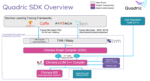
IROC products are based on a deep understanding of the soft error phenomena starting from the ionizing particles effects at transistor level and ending by the analysis of its effects on the functionality of the final system. They cover both cell level soft error simulation using TFIT, and the analysis and quantification of error propagation at circuit or SoC level using SoCFIT.
In addition to the EDA solutions, we provide radiation test services for High Energy Neutron, Thermal Neutron, Heavy Ions, Protons, Co-60, and Alpha, at the best test facilities in the world such as LANL, TRIUMF, and ISIS. We also deliver support and design consulting for management and mitigation of Soft Error Rate in complex components and systems.
What makes IROC’s EDA tools and services unique?
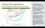
We collaborate with major foundries such as TSMC, Samsung, and Global Foundries to build accurate models for TFIT. Thanks to this collaboration, TFIT models for mainstream process nodes are built in conjunction with the foundry using process information not readily available with standard PDKs. The TFIT model for a given process characterizes the process sensitivity to ionizing particles, which can be used by TFIT to simulate any cell or custom design implemented in the target process. This unique foundry model enables TFIT to simulate the Soft Error Rate up to one hundred times (100X) faster than the best TCAD based solutions.
SoCFIT analyzes the propagation of errors from cell to system level. SoCFIT supports big designs with millions of Flip-Flops and memory blocks. The Soft Error Rate (SER) of the SoC can be calculated at high speed and mitigation solutions proposed to reduce SER with minimal area overhead.
IROC’s Test Services team has more than 20 years of experience with shuttle test campaigns, component/system test, and alpha test/count. We customize our services to our customer’s needs, from complete solutions to partial requirements. We leverage our close relationships with international testing facilities to provide the best service to our customers.
IROC also provides consulting services to customers with complex systems vulnerability analysis requirements. We use our expertise and TFIT/SoCFIT tools to provide total system error rate and identify critical parts of the design requiring reliability improvements at the cell, or SoC level.
Who is interested in your offerings?
Our customers are in the automotive, aerospace, healthcare, and HPC segments. Any semiconductor company with high reliability standards requirements can benefit from our unique foundry models, TFIT, SoCFIT, our specialized consulting, and testing services.
What are IROC’s upcoming plans?
We are continuously adding capabilities to our EDA solutions, while providing consistent high quality service offerings. We are adding new features to TFIT and SoCFIT to fit new market requirements. We will also continue to collaborate closely with foundries to add models for their latest technology process nodes.
We are working on the certification of SoCFIT according to the ISO 26262 standard and continue to investigate other safety standards that can benefit our customers concerned by functional safety.
We will soon announce our new website reflecting how our customers are using and benefiting from our unique radiation expertise and our EDA software solutions.
Visit our new website at https://www.iroctech.com/
How do customers engage with IROC?
Customers are turning to us for Soft Error analysis and mitigation using TFIT or SoCFIT and Radiation testing services. Email info@iroctech.com or visit https://www.iroctech.com/ to see how we can help you.
Also Read:
CEO Interview: Ravi Thummarukudy of Mobiveil