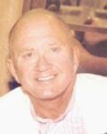
Bronco Webinar 800x100 1

A Primer on EUV Lithography

A Primer on EUV Lithography
by Fred Chen on 06-02-2023 at 6:00 am

Litho historical trend Fig 1

Extreme ultraviolet (EUV) lithography systems are the most advanced lithography systems in use today. This article is a basic primer on this important yet complex technology.

The Goal: A Smaller Wavelength

The introduction of 13.5 nm wavelength continues a trend the semiconductor industry had been following a wavelength reduction since the use of blue light (436 nm “g-line” wavelength) for feature sizes >1 micron. The light is projected through a mask (or “reticle”) which has the circuit pattern printed on it. The transmitted image is then demagnified when finally projected onto the wafer. The minimum pitch is half the wavelength divided by the numerical aperture (NA) of the system. The NA of an optical system is a dimensionless number that indicates the range of angles over which the final lens can focus light. Wavelength reduction is not trivial, as it means the energy of the photons is increased in inverse proportion. Consequently, there is high absorption in all materials. Thus, all-reflective off-axis optical systems are needed. This has led to the development of so-called “ring-field” projection systems, which lead to rotating the illumination across the exposure field [1]. Pre-EUV optical systems could rely on on-axis transmissive optics, which simplified the illumination setup by having no rotation.

A Different Mask

The use of the EUV wavelength also led to an overhaul of the mask structure. The mask is also a reflecting element. The reflection is achieved with a multilayer consisting of at least 40 molybdenum/silicon bilayers. The mask pattern uses an absorbing layer, currently based on tantalum, which is several wavelengths thick. With the off-axis illumination scattering through the absorber pattern and propagating and reflecting through the multilayer, 3D effects are inevitable in affecting the final image on the wafer [2].

The mask is also protected by a thin membrane called the pellicle, which stands off a certain distance from the mask surface. Developing a pellicle for EUV was a big deal, as light has to pass through it twice as a non-reflecting transmitting element.

Changing the Numerical Aperture

The numerical aperture in current EUV systems is 0.33. In a future generation of EUV systems, the numerical aperture will be increased to 0.55. This is expected to enable 0.6x smaller feature sizes, from the wavelength/NA proportionality. However, the depth of focus is expected to suffer by being reduced faster than the resolution, as it is roughly proportional to wavelength/(NA)^2 (Figure 1) [3]. For 0.55 NA EUV, this has led to concerns with the use of resist (the absorbing image layer on the wafer) as thin as 20 nm [4].

Figure 1. Historical trend of depth of focus vs minimum pitch [3].
A 0.55 NA system has additional complications. First, it is a half-field system, which means two mask scans are needed to fill the same area as a single mask scan in an earlier system [5]. Secondly, there is a central obscuration projected by the last two optical elements. This constrains the illumination as well as certain combinations of pitches [6]. Finally, polarization becomes important for pitches which may make use of 0.55 NA [7].

The obscuration is the fundamental systematic difference that affects projected scaling from the current 0.33 NA systems. There will be light loss just before reaching the final focusing element. In addition, the image quality will be fundamentally changed. Key components of the image diffraction spectrum. Figure 2 shows a 68 nm pitch bright line under illumination tailored for 28 nm pitch. The appearance is normal without obscuration, but with the obscuration in place, the central peak is diminished and the sidelobes beside it are enhanced, since the first diffraction order is removed. These sidelobes can print stochastically [8].

Figure 2. (Left) 68 nm pitch line under 28 nm pitch illumination, with vs. without obscuration. (Right) Stochastic sidelobe printing (top view) for the obscured case (40 mJ/cm2 absorbed) [8].
It’s Not Only the EUV Light…

EUV lithography is unfortunately plagued by a number of factors which are not obvious from the classical optical treatment so far considered. The EUV light is a form of ionizing radiation, meaning it releases electrons in the resist upon absorption. The photoelectrons (~80 eV) are from the direct ionization, and the secondary electrons are from the ionization caused by these and subsequently released electrons. The energy deposited by the electron scattering will obviously heat the resist, leading to outgassing, which will contaminate the optical elements in the EUV system. For this reason, EUV systems now contain a minimally absorbing hydrogen ambient that will keep the surfaces of the optical elements clean without oxidizing them. However, hydrogen has been known to also cause blistering [9].

Figure 3. Electron release processes following EUV photon absorption in the resist.

The electrons also spread out from the original photon absorption site, leading to the originally defined image being blurred. The effects of this blur are easily felt several nanometers away. Aggravating the spreading effect further is the inherent randomness of the entire chain of events.

EUV Reveals the Stochastic Nature of Lithography

Photon absorption and electron scattering are all inherently random events. These lead to CD non-uniformity and edge roughness, and even placement errors and serious defects. Stochastic effects are more serious with lower absorbed photon density. Thinner resists reduce absorption, enhancing this effect. However, increased photon density leads to increased electron number density and increased electron blur, whose randomness leads to stochastic defects [10]. DUV lithography had not dealt with stochastic issues mainly because the feature sizes were large enough to secure enough photons, but EUV could not exploit this benefit.

References
  1. Antoni et al., Proc. SPIE 4146, 25 (2000).
  2. Tanabe, Proc. SPIE 11854, 1185416 (2021).
  3. J. Lin, J. Micro/Nanolith., MEMS, and MOEMS 1, (2002).
  4. https://www.imec-int.com/en/articles/high-na-euvl-next-major-step-lithography
  5. Davydova et al., Proc. SPIE 12494, 124940Q (2023).
  6. https://www.youtube.com/watch?v=1HV2UYABh4E
  7. https://www.youtube.com/watch?v=agMx-nuL_Qg
  8. https://www.youtube.com/watch?v=sb46abCx5ZY
  9. https://www.youtube.com/watch?v=FZxzwhBR5Bk&t=3s
  10. https://www.linkedin.com/pulse/secondary-electron-blur-randomness-origin-euv-stochastic-chen

Also Read:

SPIE 2023 – imec Preparing for High-NA EUV

Curvilinear Mask Patterning for Maximizing Lithography Capability

Reality Checks for High-NA EUV for 1.x nm Nodes


Securing PCIe Transaction Layer Packet (TLP) Transfers Against Digital Attacks

Securing PCIe Transaction Layer Packet (TLP) Transfers Against Digital Attacks
by Kalar Rajendiran on 06-01-2023 at 10:00 am

PCIe TLP Encryption

In the fast moving world of data communications, the appetite for high speed data transfers is accompanied by a growing need for data confidentiality and integrity. The wildly popular PCIe interface standard for connectivity has not only been increasing data transfer rates but has also introduced an Integrity and Data Encryption (IDE) security option. The introduction of IDE features in PCIe enables the processing of higher data bandwidths while encrypting the data to maintain its integrity.

Siemens EDA has a published a whitepaper that discusses the encryption flow used in IDE Transaction Layer Packets (TLPs) in PCIe and the underlying software stack. The paper explains how IDE ensures security against digital attacks on TLPs transferred from the transmitter to the receiver, including link-to-link connections and devices connected through switches. The TLPs are encrypted using keys exchanged during IDE key management. Furthermore, the whitepaper explains the underlying protocols used in IDE, including data object exchange (DOE), component measurement and authentication (CMA), and security protocol and data model (SPDM).

Data Object Exchange (DOE)

Data Object Exchange (DOE) in PCIe is an extended capability introduced to transfer various types of data objects between devices. Each vendor can define specific data objects, which are identified by a vendor ID assigned by PCI-SIG. Data are transferred as data objects, one double word (32-bits) at a time, forming packets through configuration write transactions in PCIe. The transmitting device sets the DOE go bit after sending the entire length of the data object. The receiving device consumes the data and begins forming a response. Once the response is ready, the receiving device sets the DOE data object ready bit in its configuration space. The transmitter reads the response one double word at a time until the data object ready bit is high. This process enables the transfer of data from one device to another.

Component Measurement and Authentication (CMA)

The Component Measurement and Authentication (CMA) feature in PCIe relies on the underlying Security Protocol and Data Model (SPDM) protocol. CMA utilizes the DOE feature to transfer packets for secure connection establishment. Within the CMA/SPDM framework, the authenticity of connected devices is verified using digital signatures and public key cryptography. This process ensures that the devices involved in the connection are genuine and trusted. Once the authenticity of the connected devices is established, a secure connection is formed between the requester and responder. The secure CMA/SPDM protocol is then utilized to transfer data objects securely. The data objects are transmitted using the negotiated algorithm that was employed during the establishment of the secure connection.

IDE Key Management

IDE key management is used to exchange keys that will be utilized to encrypt IDE TLPs. The process involves exchanging keys on a per sub-stream basis for both transmitting and receiving TLPs. There can be two sets of keys identified by the K bit in the IDE prefix, with each set containing different keys for the Tx and Rx directions. There are seven different types of packets involved in the IDE key management process, each identified by an object ID field. The full details are described in the whitepaper.

Integrity and Data Encryption (IDE)

The goal of securing data transfers is to not only prevent unauthorized access but also to prevent tampering. Even with encryption, it is possible that attackers may be able to modify the data without the receiver’s knowledge unless there is a check for data integrity. The Message Authentication Code (MAC) feature of the IDE mechanism makes data integrity check possible. A secure state is achieved through the establishment of a secure connection using CMA/SPDM, configuration of keys using IDE key management, and enabling IDE by setting the IDE enable bit. The whitepaper goes into details of the transmit-receive data flow and the Advanced Encryption Standard-Galois/Counter Mode (AES-GCM) encryption/decryption process using keys and initialization vectors. Based on the MAC check, an IDE stream can be marked as being in secure state or insecure state. An IDE stream can transition from secure to insecure state if the security condition is compromised.


The IDE mechanism also provides flexibility in securing TLP transfers. The establishment of an IDE stream between two ports can be accomplished by connecting using Link IDE or Selective IDE. When a switch is present between the ports, selective IDE is used to encrypt the packets transferred between them. Link IDE and selective IDE can work independently or together for directly connected ports.

Verification of IDE Feature with Siemens EDA’s Questa VIP

Siemens QVIP serves as a comprehensive verification solution offering support for the entire IDE feature verification process. It includes stimulus generation, assertion checks, error injection capabilities, and extensive sequence libraries. The presence of debug and log features further enhances the efficiency and effectiveness of the verification process.

Summary

The whitepaper also goes into details of IDE TLP prefixes (M-bit, K-bit, T-bit and P-bit) and what purpose they serve. For example, the presence of the M bit in an IDE prefix indicates whether a MAC is present or not. The paper also covers TLP aggregation that allows multiple TLPs to be combined into a single unit for transmission for achieving increased throughput.

The whitepaper will be a valuable read for anyone involved in implementing data integrity and security for PCIe-based systems.

Also Read:

Emerging Stronger from the Downturn

Chiplet Modeling and Workflow Standardization Through CDX

Tessent SSN Enables Significant Test Time Savings for SoC ATPG


WEBINAR: Driving Forward with UWB Radar: Enhancing Child Safety in Automotive

WEBINAR: Driving Forward with UWB Radar: Enhancing Child Safety in Automotive
by Daniel Nenni on 06-01-2023 at 6:00 am

CEVA UWB Radar Webinar Email Invitation 230521


The rapid advancement of UWB (Ultra-Wideband) wireless technology has garnered significant attention and interest, thanks to its adoption by leading smartphone brands and its versatile range of applications. Within the automotive industry, UWB has already emerged as the preferred choice for Digital Keys in the premium segment. Moreover, the integration of UWB anchor points in modern vehicles presents a cost-effective platform for implementing advanced in-cabin radar capabilities, particularly for Child Presence Detection (CPD). This webinar aims to provide valuable insights into UWB technology, its functionality, and the role it plays in improving child safety in automotive environments.

Register Here

UWB Technology and Ecosystem

To comprehend the potential of UWB radar in automotive applications, it is essential to understand the underlying technology and the ecosystem surrounding it. The UWB Alliance, CCC (Car Connectivity Consortium), and FiRa (Fine Ranging) are key players in promoting UWB technology. The UWB Alliance fosters collaboration and innovation among industry leaders, driving the development and adoption of UWB solutions across various sectors. CCC focuses on standardizing the implementation of UWB technology in vehicles, ensuring interoperability and seamless integration with other connected car technologies. FiRa, on the other hand, is dedicated to advancing UWB’s precise positioning capabilities, enabling enhanced location-based services.

How UWB Radar Works

UWB radar leverages the unique characteristics of ultra-wideband signals to enable accurate and reliable detection and ranging. UWB signals consist of extremely short pulses with a wide frequency spectrum, allowing for high-resolution sensing. By transmitting these pulses and analyzing the reflections, UWB radar can identify and locate objects with exceptional precision. This technology excels in differentiating between closely spaced objects and can operate effectively in challenging environments with high levels of interference.

CEVA’s UWB and Radar Solutions

CEVA, a leading provider of wireless connectivity and smart sensing technologies, offers cutting-edge UWB and radar solutions for automotive applications. During the webinar, participants will gain insights into CEVA’s UWB technology, which provides secure and accurate positioning for digital key solutions. CEVA’s radar solutions leverage UWB technology to enable advanced in-cabin features such as Child Presence Detection. By integrating UWB radar into vehicles, automakers can enhance child safety by detecting the presence of a child within the car. Additionally, UWB technology enables new features based on gesture recognition, such as opening the trunk with a simple hand gesture.

Target Audience

This webinar is designed to benefit system engineers, SoC (System-on-Chip) designers, and product managers who are involved in UWB device development and are interested in incorporating radar capabilities into their products. Professionals from diverse industries, including automotive, industrial, consumer electronics, and others, will find this webinar valuable for understanding the potential applications of UWB radar and its role in enhancing safety and convenience in their respective domains.

Conclusion

As UWB wireless technology gains traction across various industries, its implementation in the automotive sector holds immense potential, particularly in improving child safety. The integration of UWB anchor points in modern vehicles creates a cost-effective platform for deploying advanced in-cabin radar systems, enabling features like Child Presence Detection. This webinar offers a comprehensive overview of UWB technology and its ecosystem, provides insights into the working principles of UWB radar, and showcases CEVA’s UWB and radar solutions for automotive applications. By attending this webinar, participants will gain valuable knowledge and perspectives on leveraging UWB radar to enhance child safety and drive innovation in the automotive industry.

Register Here

Also Read:

DSP Innovation Promises to Boost Virtual RAN Efficiency

All-In-One Edge Surveillance Gains Traction

CEVA’s LE Audio/Auracast Solution

CEVA Accelerates 5G Infrastructure Rollout with Industry’s First Baseband Platform IP for 5G RAN ASICs


Real-Time AI-driven Image Signal Processing with Reduced Memory Footprint and Processing Latency

Real-Time AI-driven Image Signal Processing with Reduced Memory Footprint and Processing Latency
by Kalar Rajendiran on 05-31-2023 at 10:00 am

AI ISP for Automotive, Low Light Image Enhancement

In our day to day lives, we all benefit from image signal processing (ISP), whether everyone realizes it or not. ISP is the technique of processing image data captured by an imaging device. It involves a series of algorithms that transform raw image data into a usable image by correcting for distortions, removing noise, adjusting brightness and contrast, and enhancing features. So, ISP by itself is not something new.

What is new though is leveraging artificial intelligence (AI) to enhance ISP to yield better results than traditional ISP can. Firstly, in the field of digital photography, AI can significantly enhance ISP capabilities. Traditional ISPs are effective at processing images, but AI can take this to the next level. For instance, AI can help in noise reduction, improving the image’s clarity, especially under low-light conditions. Moreover, AI algorithms can recognize various scenes or objects in the image, enabling automatic adjustments to different parameters like brightness, contrast, and saturation for optimal results.

In the world of autonomous vehicles, AI-enhanced ISPs can process real-time images to understand the vehicle’s surroundings better, aiding in decision-making. Traditional ISPs can struggle with different lighting conditions or object detection at high speeds, but AI can improve upon these aspects, enhancing the vehicle’s ability to react to potential hazards and improve overall road safety.

Lastly, in the realm of surveillance and security, AI-enhanced ISPs can process images from CCTV footage more effectively. AI can help detect suspicious activities, recognize faces, or identify objects left unattended, providing real-time alerts and enhancing overall security measures.

But how to implement AI-based ISP? It is easier said than done. There are a lot of challenges to overcome.  AI algorithms are fast advancing, requiring an AI-ISP solution to be programmable. AI models require a lot of computational power. Conventional  techniques combining separately developed ISP and NPU often require a lot of memory to store entire frames of images for processing. Accessing DDR-SDRAMs consume a lot of power. And this loosely coupled frame-based solution will introduce latencies measured in frames, which is unacceptable for many applications.

What is needed for today’s applications is real-time processing at low latency and low power consumption. Making the solution DDR-less is even more attractive as it will reduce the system power requirements significantly. Of course, NPUs are key to an AI-based ISP solution. But there is a lot more to arriving at a DDR-less, low latency, low power AI-ISP solution. This was the topic of Mankit Lo’s presentation at the recent Embedded Vision Summit conference. Mankit, who is the Chief Architect, NPU IP Development at VeriSilicon walked the audience through the various aspects that need to be addressed.

Solution Requirements

ISP Requirements

In traditional hardware for ISP, there are many modules in the pipeline stages to correct the potential artifacts of the imaging system. To perform AI-ISP, the chosen ISP should be flexible enough to allow the customer to pick and choose the modules to replace or enhance.

NPU Requirements

As ISP tasks are computationally huge and intense, the task is usually partitioned to be executed on many NPU cores. There is a lot of image overlap on the input side going into the NPU cores. Even for a 3×3 convolution layer inside the neural network, the overlapping requirement for just a few pixels could result in a huge overlap at the whole network level. The overlap needs to be minimized for reducing the memory, power, and computing demand on the system. The way to do it is through layer-level overlap sharing.

What is needed is an NPU that can handle raster lines and become part of the ISP processing pipeline, making the solution DDR-less, low latency, and low power. The NPU needs to be programmable to handle a changing AI network model landscape and deliver very good performance. It also needs to be able to support Per Layer Overlap Sharing which results in not requiring any overlap on the image input side.

VeriSilicon Offers

Specific to the topic of AI-ISP, VeriSilicon provides ISP, NPU, and the FLEXA-PSI interface to seamlessly connect these IPs. Refer to the block diagram of a VeriSilicon AI-ISP solution.

The customers need to just add their custom AI algorithms to the mix to complete their unique solution. VeriSilicon can also provide algorithms relating to the ISP such as noise reduction, demosaicing, and different types of detection such as facial detection and scene detection, etc.

Click here to learn more about VeriSilicon’s NPU IP offering.

Click here to learn more about VeriSilicon’s ISP IP offering.

VeriSilicon offers custom silicon services and a very broad portfolio of IP for many different markets. Learn more at VeriSilicon.com

Also Read:

VeriSilicon’s VeriHealth Chip Design Platform for Smart Healthcare Applications

VeriSilicon’s AI-ISP Breaks the Limits of Traditional Computer Vision Technologies


Investing in a sustainable semiconductor future: Materials Matter

Investing in a sustainable semiconductor future: Materials Matter
by Daniel Nenni on 05-31-2023 at 6:00 am

EMD LinkedIn Twitter Materials Matter

In 2020 TSMC established its Net Zero Project with a goal of net zero emissions by 2050. I remember wondering how could this possibly be done before 2050 or at all for that matter. After working with TSMC for 20+ years I have learned never to bet against them on any topic and green manufacturing is one of them, absolutely.

TSMC presented on green manufacturing at the recent symposium in Silicon Valley. Clearly energy and water resources are critical parts of any net zero project but carbon emissions are also a of great importance and that means materials. In regards to semiconductor manufacturing materials we have experts here on SemiWiki.

EMD Electronics has a presence in 66 countries and over 100 years of invaluable experience in the electronic materials space delivering a broad portfolio of semiconductor and display materials for cutting-edge electronics.

EMD Electronics recently published a paper: INVESTING IN A SUSTAINABLE SEMICONDUCTOR FUTURE – MATERIALS MATTER.

It is a very interesting comprehensive look at innovative sustainable semiconductor materials techniques that decrease carbon emissions, improve resource efficiency and productivity, and highly contribute to achieving net zero semiconductor.

“It is amazing where collaboration can take us. Sustainability is no longer the result of individuals; only by working together can we get closer to our goals for a sustainable future! Brita Grundke, Head of Sustainability, EMD Electronics”

Here is the introduction. This paper is freely available and well worth the read for semiconductor professionals at all levels:

Emissions from semiconductor manufacturing are a growing segment of global greenhouse gas (GHG) emissions. There are two reasons behind this trend. First, the demand for semiconductor chips is growing. Our technology appears in everything from mobile phones to automobiles, where the number of chips per vehicle increases every year. Data storage, which relies on the semiconductor industry, is exploding. Second, today’s manufacturing processes have more deposition and etch steps than ever. Each step consumes water and electricity and creates GHG emissions.

Semiconductor companies large and small talk about achieving climate neutrality by 2030. That sounds like a great goal. But merely achieving that goal won’t solve the emissions problem. How we get there matters.

Buying carbon offsets is an easy way out. It isn’t the best long-term answer, because many offsets are not as effective as they claim to be. Some may even make the problem worse, defeating the purpose [1]. And relying on offsets can make internal actions seem less pressing. It is best to see offsets as a temporary or last-choice option.

Semiconductor industry leaders are, of course, doing more than buying offsets. They are investing in renewable energy, improving the energy efficiency of their processes, and finding ways to reduce waste. These actions are helpful, and we must do more. Despite modest success in reducing emissions per wafer or per revenue, demand for semiconductor chips is growing faster than the improvements can handle. We need more drastic reductions, and that starts by examining the sources.

Bottom Line: Climate change is real and semiconductor manufacturing is under a microscope now that it is being regionalized due to the shortages and supply chain issues we suffered during the pandemic. If you really want to know why semiconductor manufacturing left the US it was due to the Environmental protection Agency crack down on water, ground, and air pollution. I grew up in Silicon Valley so I had front row seat to the environmental issues of semiconductor manufacturing. Now that semiconductor manufacturing is coming back to the US and other parts of the world sustainability is front and center once again.

Also Read:

Step into the Future with New Area-Selective Processing Solutions for FSAV

Integrating Materials Solutions with Alex Yoon of Intermolecular

Ferroelectric Hafnia-based Materials for Neuromorphic ICs


Coherent Optics: Synergistic for Telecom, DCI and Inter-Satellite Networks

Coherent Optics: Synergistic for Telecom, DCI and Inter-Satellite Networks
by Kalar Rajendiran on 05-30-2023 at 10:00 am

Data Connectivity to the Edge

The telecommunications industry has experienced significant growth in recent years, driven by the increasing demand for high-speed internet and data services. This growth has created a surge in traffic on optical networks, leading to the development of new telecom network architectures that can support the increasing demand for bandwidth.

Optical networking technologies, such as coherent optics, have traditionally been developed for telecom applications. However, with the growth of hyperscale data centers and the increasing demand for high-speed networking, these technologies are now also being adopted in data center applications. Traditionally, data centers have used copper or short-range optical cables to connect servers and storage devices within the same data center. However, as data volumes continue to grow and data center interconnect (DCI) requirements increase, coherent optical networking is becoming an attractive option for data centers. With coherent optical networking, data centers can achieve higher data transmission rates over longer distances, resulting in increased data capacity and lower latency. 400G was the first data rate where hyperscale data center applications outpaced telecom applications in the use of coherent optics.

Coherent optics enables the transmission of high-speed data over long distances by using advanced signal processing techniques to mitigate the effects of signal distortion and noise. This technology is essential for supporting the growing demand for high-speed internet and data services, particularly in areas where traditional copper-based networks are not feasible. This trend is likely to continue and proliferate further going forward, driven by the ongoing growth of cloud computing, big data, AI/ML workloads and other data-intensive applications.

Another driver of the shift towards optical interconnects has been the increasing complexity of satellite networks. As satellite networks become more complex, the need for high-speed, low-latency communication between satellites becomes more important. Optical interconnects are ideal for this type of communication, as they offer very low latency and can support high-speed data transfer between satellites.

Optical Telecom – Satellite Communications Synergies

Optical telecom synergies have played a significant role in the evolution of inter-satellite communication. Many of the technologies and techniques used in optical telecom networks have been adapted for use in inter-satellite communication. Innovations in optical digital signal processing (DSP) and system automation also offer several optimization opportunities with inter-satellite interconnects.

Improved Signal Quality: Optical DSP can be used to compensate for impairments in the optical signal, such as chromatic dispersion and polarization mode dispersion. This can improve the quality of the signal and reduce the bit error rate (BER), enabling high-quality communications over long distances.

Reduced Latency: System automation can also be used to optimize the routing of data between satellites, minimizing the number of hops and reducing latency. This can improve the responsiveness of the system and enhance the user experience.

Power-efficient Modulation Formats: Optical DSP can enable the use of power-efficient modulation formats, such as pulse-amplitude modulation (PAM), which can reduce the power consumption of the inter-satellite links while maintaining high data rates.

Energy-efficient Signal Processing: Optical DSP can also be optimized to perform signal processing operations more energy-efficiently. For example, parallel processing and low-power digital signal processing techniques can reduce the power consumption of the signal processing circuitry.

Interoperability Demonstration

At the recent Optical Fiber Communication (OFC) conference, Alphawave Semi showcased its ZeusCORE XLR test chip during the interoperability demonstration organized by the Optical Internetworking Forum (OIF). Alphawave Semi executives Loukas Paraschis, VP of Business Development and Tony Chan Carusone, CTO, presented on high-speed connectivity leadership. Their presentations touched on the growing synergies and optimization opportunities of inter-satellite interconnects and optical telecom through innovations in optical DSP and system automation.

Summary

As the volume of data traffic on optical networks continues to increase, it is essential to ensure that the cost of implementing and maintaining these networks remains affordable. This requires a delicate balance between increasing volume and decreasing costs, which can only be achieved through innovation and the development of highly-integrated co-designed solutions. These solutions combine multiple technologies and functions into a single device, reducing the complexity and cost of optical network infrastructure. This approach enables the development of more efficient, cost-effective optical networks that can meet the growing demand for bandwidth and high-speed data transmission.

To learn more about the ZeusCORE, visit the product page.

Also Read:

Alphawave Semi Showcases 3nm Connectivity Solutions and Chiplet-Enabled Platforms for High Performance Data Center Applications

Alphawave Semi at the Chiplet Summit

Alphawave IP is now Alphawave Semi for a very good reason!


Deep Learning for Fault Localization. Innovation in Verification

Deep Learning for Fault Localization. Innovation in Verification
by Bernard Murphy on 05-30-2023 at 6:00 am

Innovation New

A new look at fault localization and repair in debug using learning based on deep semantic features. Paul Cunningham (Senior VP/GM, Verification at Cadence), Raúl Camposano (Silicon Catalyst, entrepreneur, former Synopsys CTO and now Silvaco CTO) and I continue our series on research ideas. As always, feedback welcome.

The Innovation

This month’s pick is Improving Fault Localization and Program Repair with Deep Semantic Features and Transferred Knowledge. The authors presented the paper at the 2022 International Conference on Software Engineering and are from Beihang University in Beijing and Newcastle University in New South Wales.

The method goes beyond familiar spectrum-based (SBFL) and mutation-based (MBFL) localization techniques to use deep learning from pre-qualified datasets of bugs and committed fixes. The fix aspect is important here because it depends on very accurate localization of a fault (in fact localization and nature of the fix are closely linked). The paper uses SBFL and MBFL metrics as input to their deep learning method. The authors demonstrate their methods are more effective than selected SBFL and MBFL approaches and argue this is because other methods have either no semantic understanding or only a shallow understanding of semantic features of the design, whereas they intentionally have a deeper understanding.

Fully automatic repair might be a step too far for RTL debug, however suggested fixes are already familiar for spell and grammar checks, hinting that this feature might also be valuable in verification.

Paul’s view

One year on from our review of DeepFL, we take a look at another paper that tries to move the needle further. Automatic bug detection is now a regular topic with Cadence customers and expectations are high that deep neural networks or large language models can be used to dramatically improve time spent root causing bugs.

DeepFL used a RNN to rank code for bugs based on suspiciousness features (complexity-based, mutation-based, spectrum-based, text-based). This month’s paper adds an additional bug template matching step as a further input feature to improve accuracy. The bug template matcher is itself another RNN that matches individual code statements to one or more of 11 possible bug templates, e.g. a missed null pointer checker, incorrect type cast, incorrect statement position, or incorrect arithmetic operator.

The key contribution of the paper for me is the dataset the authors build to train their bug template matching network. They mine the entire github repository to find real bug fixes that match their bug templates. For each match they require that there be another matching statement elsewhere in the same source code file that is not part of the bug fix – i.e. so the dataset has both positive and false-positive matches. The final dataset has around 400,000 positive/false-positive bug fix pairs. Nice!

As with DeepFL, the authors benchmark their tool TRANSFER-FL using Defects4J. Results look decent – 171 of the 395 bugs in Defects4J are ranked Top-5 by TRANSFER-FL vs. 140 using DeepFL. However, from a commercial standpoint 171 is still less than half of the total 395 benchmark set. If you look at the average rank across all 395 it’s 80, a long way from Top-5, so a ways off commercial deployment. I’m looking forward to reviewing some large language model-based papers next year that move the needle yet further 😊

Raúl’s view

This month we move into the areas of fault localization and automatic program repair for SW, the reviewed paper explores these techniques for Java code. In May 2022 we reviewed DeepFL, which is similar to this paper in that it extends traditional spectrum- and mutation-based techniques for fault localization with deep learning models.

To state my conclusion upfront, perhaps automatic RTL or SystemC fault localization and code repair will become routine in the foreseeable future… The authors are optimistic regarding the applicability to other languages, “most of the fix templates can be generalized to other languages because of the generic representation of AST (Abstract Syntax Tree)” with the caveat that sufficient data needs to be available for training the different networks used in their approach. For the paper 2000 open-source Java projects from GitHub were collected to construct 11 fault localization datasets with a total of 392,567 samples (faulty statements for 11 bug types that have a bug fix commit); and a program repair dataset with 11 categories of bug fixes with a total of 408,091 samples, each sample consisting of a faulty statement with the contextual method and its corresponding bug type. An AST is used to do this matching.

The detailed approach, called TRANSFER, is rather complex and requires some time to digest, 67 references help to dive into the details. It leverages existing approaches for fault localization, 1) Spectrum-based features which take source code and relevant test cases as inputs and output a sorted list of code elements ordered by suspicion scores calculated from the execution of test cases, and 2) Mutation-based features which calculate suspicion scores by analyzing the changes of execution results between original code element and its mutants. It adds 3) Deep Semantic features obtained by using BiLSTM (Bidirectional Long Short-Term Memory) binary classifiers trained with the fault localization datasets. Program repair is done using a “fine-tuned” multi-classifier trained with the program repair dataset.

The bottom line is that TRANSFER outperforms existing approaches, successfully fixing 47 bugs (6 more than the best existing approaches) on the Defects4J benchmark.

Writing and debugging SW is already routinely assisted by AI such as GitHub Copilot; designing hardware, aka writing RTL or higher-level code, can’t be too far behind, perhaps the largest obstacle being the availability of the data required.

Also Read:

Opinions on Generative AI at CadenceLIVE

Takeaways from CadenceLIVE 2023

Anirudh Keynote at Cadence Live


WEBINAR: An Ideal Neural Processing Engine for Always-sensing Deployments

WEBINAR: An Ideal Neural Processing Engine for Always-sensing Deployments
by Daniel Nenni on 05-29-2023 at 10:00 am

Option 1

Always-sensing cameras are a relatively new method for users to interact with their smartphones, home appliances, and other consumer devices. Like always-listening audio-based Siri and Alexa, always-sensing cameras enable a seamless, more natural user experience. However, always-sensing camera subsystems require specialized processing due to the quantity and complexity of data generated.

But, how can always-sensing sub-systems be architected to meet the stringent power, latency, and privacy needs of the user? Despite ongoing improvements in energy storage density, next-generation devices always place increased demands on batteries. Even wall-powered devices face scrutiny, with consumers, businesses, and governments demanding lower power consumption. Latency is a huge factor as well; for the best user experience, devices must instantly react to user inputs, and always-sensing systems cannot compete with other processes which add unneeded latency and slow reasons. Privacy and data security are also significant concerns; always-sensing systems need to be architected to securely capture and process data from the camera without storing or exposing it.

So how can always-sensing be enabled in a power, latency, and privacy-friendly method? While many existing Application Processors (APs) have NPUs inside of them, those NPUs aren’t the ideal vehicle for always-sensing. A typical AP is a mix of heterogeneous computing cores, including CPUs, ISPs, GPU/DSPs, and NPUs. Each processor is designed for specific computing and potentially large processing loads. For example, a typical general-purpose NPU might provide 5-10 TOPS of performance, with a typical power consumption of around 4 TOPS/W and about 40% utilization. However, it is inefficient because it must be somewhat overdesigned to handle worst-case workloads.

Always-sensing neural networks are specifically created to require minimal processing, typically measured in GOPS — GOPS being one-thousandth of TOPS. While the NPU in an existing AP is capable of always-sensing AI processing, it’s not the right choice for various reasons. First, power consumption will significant, which is a non-starter for an always-on feature since it translates directly to reduced battery life. Second, since AP-based NPU is typically busy with other tasks, other processes can increase latency and negatively impact the user experience. Finally, privacy concerns essentially preclude using the application processor. This is because the always-sensing camera data needs to be isolated from the rest of the system and must not be stored within the device or transmitted off the device. This is necessary to limit the exposure of that data and reduce the chances of a nefarious party stealing the data.

The solution, then, is a dedicated NPU specifically designed and implemented to process always-sensing networks with an absolute minimum of area, power, and latency: the LittleNPU.

In this webinar, Expedera and SemiWiki explore how a dedicated always-sensing subsystem with a dedicated LittleNPU can address the power, latency, and privacy needs while providing an incredible user experience.

REGISTER HERE

Presented by
Sharad Chole, Expedera Chief Scientist and Co-founder

About this talk
Always-sensing cameras are emerging in smartphones, home appliances, and other consumer devices, much like the always-listening Siri or Google voice assistants. Always-on technologies enable a more natural and seamless user experience, allowing such features as automatic locking and unlocking of the device or display adjustment based on the user’s gaze. However, camera data has quality, richness, and privacy concerns which requires specialized Artificial Intelligence (AI) processing. However, existing system processors are ill-suited for always-sensing applications.

Without careful attention to Neural Processing Unit (NPU) design, an always-sensing sub-system will consume excessive power, suffer from excessive latency, or risk the privacy of the user, all leading to an unsatisfactory user experience. To process always-sensing data in a power, latency, and privacy-friendly manner, OEMs are turning to specialized “LittleNPU” AI processors. In this webinar, we’ll explore the architecture of always-sensing, discuss use cases, and provide tips for how OEMs, chipmakers, and system architects can successfully evaluate, specify, and deploy an NPU in an always-on camera sub-system.

About Expedera
Expedera provides scalable neural engine semiconductor IP that enables major improvements in performance, power, and latency while reducing cost and complexity in AI-inference applications. Third-party silicon-validated, Expedera’s solutions produce superior performance and are scalable to a wide range of applications from edge nodes and smartphones to automotive and data centers. Expedera’s Origin™ deep learning accelerator products are easily integrated, readily scalable, and can be customized to application requirements. The company is headquartered in Santa Clara, California. Visit expedera.com
Also Read:

Deep thinking on compute-in-memory in AI inference

Area-optimized AI inference for cost-sensitive applications

Ultra-efficient heterogeneous SoCs for Level 5 self-driving

CEO Interview: Da Chuang of Expedera


Why Secure Ethernet Connections?

Why Secure Ethernet Connections?
by Daniel Payne on 05-29-2023 at 6:00 am

Ethernet Security min

While web browsing I constantly glance for the padlock symbol to indicate that the site is encrypting any of my form data by using the https prefix, which means that an SSL (Secure Sockets Layer) certificate is being used by the web hosting company. I have peace of mind knowing that my credit card information cannot be easily stolen on secure web sites using an SSL certificate. For Ethernet networks there are also several potential security breaches:

  • Man-in-the-middle attacks
  • Eavesdropping
  • Denial of service
  • Privilege escalation

The downside risks of data theft are quite high to any organization, and being compliant with data security standards like Health Insurance Portability and Accountability Act of 1996 (HIPAA) in the US and the  General Data Protection Regulation (GDPR) are important.

To detect and prevent any unwanted data intrusions a system must have privacy measures like source validation and authentication.

Secure Ethernet Protocol

Thankfully, the IEEE created the Media Access Control Security (MACsec) protocol in 2006 to help secure Ethernet networks. The cryptography used to protect Ethernet traffic in MACsec is  Advanced Encryption Standard-Galois/Counter Mode Cryptography (AES-GCM), also used for CXL and PCI Express security. MACsec is applied at Layer 2 of the Open Systems Interconnection (OSI) networking model, enabling data integrity, confidentiality, replay protection and data origin authenticity.

MACsec uses AES-GCM cryptography

The encrypted connection with MACsec has several authentication steps:

  1. A Pre-Shared Key (PSK) for mutual peer authentication.
  2. A secure Connectivity association Key Name (CKN) is exchanged.
  3. The two endpoints decide which is the key server, and key client.
  4. The key server sends the Secure Association Key (SAK) to the key client.
  5. Encrypted data is ready for exchange.

You could take the time to become an expert on MACsec and design your own Ethernet security solution that conforms to the protocol, or consider using Ethernet IP from Synopsys that in addition to controllers and PHYs includes their MACsec Security Modules. Here’s what the Ethernet security IP from Synopsys looks like:

Synopsys Ethernet Solution with MACsec security

The benefits of using the Synopsys MACsec Security Modules include compliance with the IEEE 802.1AE standard, throughput scalability and configurability to tune solutions for specific applications and use cases with optimal latency, power, performance and area.

Synopsys not only has secure IP for Ethernet, it also extends into other interfaces: PCIe, CXL, USB, HDMI, DisplayPort, DDR, LPDDR, Die-to-Die, MIPI, UFS and eMMC.

Synopsys Secure Interfaces Solutions

Kalar Rajendiran wrote more about this topic in his January blog on SemiWiki.

Summary

Having a secure Ethernet makes a lot of sense, and with the IEEE protocol MACsec there’s a standard way to ensure that network data is not stolen or compromised. Malicious actors want to steal our web browsing activity and that extends into the realm of Ethernet traffic.

Instead of waiting to have your Ethernet data breached, why not be proactive by adding the MACsec protocol in your SoC implementation. Do the math on the cost of building your own MACsec compliant IP, then compare that to what Synopsys has designed and verified already. The semiconductor IP industry has grown steadily for many years now, and for good reason, IP blocks from a trusted vendor can offer a faster path to market while not requiring your engineering team to become domain experts in something new and unfamiliar.

Related Blogs


Podcast EP164: How Weebit Nano is Disrupting the Memory Market with Coby Hanoch

Podcast EP164: How Weebit Nano is Disrupting the Memory Market with Coby Hanoch
by Daniel Nenni on 05-26-2023 at 10:00 am

Dan is joined by Coby Hanoch, Coby joined Weebit Nano as CEO in 2017. He has 15 years of experience in engineering and engineering management roles, and 28 years of experience in sales management and executive roles.

Coby explains the unique features of Weebit Nano’s non-volatile ReRAM technology. He explores the technology’s extended compatibility across advanced process nodes and its speed and power advantages as compared to more traditional approaches such as flash. He discusses current and future deployment for both embedded and discrete applications.

The views, thoughts, and opinions expressed in these podcasts belong solely to the speaker, and not to the speaker’s employer, organization, committee or any other group or individual.