
System architects have a difficult task of choosing the most efficient architecture by exploring alternative approaches, while tracking and testing requirements. Using a Model-Based Systems Engineering (MBSE) approach is recommended to achieve these goals, before getting mired in low-level implementation details like RTL code. Mirabilis is an EDA vendor at DAC this year that aims at using an MBSE methodology through their VisualSim tool. I spoke with Deepak Shankar, founder of Mirabilis Design by phone this week to get a preview of what they’re doing at DAC.
The three big messages from Mirabilis this year for DAC that will interest system architects are:
1. Integration with Model Based Systems Engineering
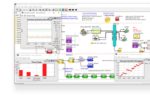
Architects can import their existing SysML models into the VisualSim tool. The adoption of SysML started out in the Defense community and now even system-level semiconductor companies are using it. SysML can manage your code, but it cannot predict what the performance and power will be when mapping to HW like an SoC. SysML cannot tell cache contention, because there is no latency understanding. Using VisualSim with MBSE supplies the requirements data, allowing you to measure latency, see the buffer occupancy, and even track radiation requirements.
2. Addition of RISC-V modeling environment
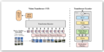
RISC-V is a very popular Instruction Set Architecture (ISA) that can be extended for specific domains, but how would you do power and performance comparisons between using SiFive or an ARM architecture? How about system-level benchmarks?
With Mirabilis there are pre-built models of RISC-V IP, plus you can even create your own special RISC-V architecture. For Network On Chip (NoC) you can choose from models for Arteris NoC or ARM NoC. In VisualSim Architect you can run benchmarks for RISC-V, and see what would happen if your data is stored in cache or you have to use external RAM. You can also see the performance and identify your architectural bottlenecks. This analysis allows you to evaluate RISC-V cores for use inside an SoC, or model an SoC to give to customers so they can start planning the architecture of their end products. VisualSim allows an engineer to understand pipelines and the entire system all in one platform.
3. Created a new packaging mechanism
A RISC-V core vendor could package their high-level model before product development even starts, to use it inside an SoC, then hand it off to their end customer to see how the full system works. A semiconductor vendor, tier 1 supplier and customer can all be sharing the same executable models. Denso is an example customer sharing models of their auto ECUs as a tier 1 supplier for automotive companies, and they saved 40% of development time by using VisualSim.
DAC Paper
Mirabilis has a DAC paper on system modeling and failure analysis in avionics, in conjunction with a US Defense application.
Attend this presentation on Tuesday, July 11th, from 2:24pm – 2:42pm PDT, room 2008 on Level 2, as part of the Embedded Systems and Software track.
DAC Booth
You will find Mirabilis in booth #2217, that’s on the 2nd floor at Moscone West, and in their booth will be three technical people to speak with. While other vendors tend to only show PowerPoint slides, you will instead see a live demo of the VisualSim Architect tool in action, now that’s confidence.
You may also sign up for a private discussion in their suites by requesting online here.
Summary
System design and system modeling has become much easier, is accurate, and by using system-level IP your system architects will analyze quickly and explore more thoroughly than with other methods. At this level of abstraction your team can analyze and uncover architectural bottlenecks before detailed RTL implementation starts.
Enjoy some chocolate at the booth, I’ve heard that it’s quite tasty.


