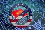
Bronco Webinar 800x100 1

Sirius Wireless Partners with S2C on Wi-Fi6/BT RF IP Verification System for Finer Chip Design

Sirius Wireless Partners with S2C on Wi-Fi6/BT RF IP Verification System for Finer Chip Design
by Daniel Nenni on 08-17-2023 at 10:00 am

Picture

Sirius Wireless, a provider of RF IP solutions, collaborated with FPGA prototyping solutions expert S2C to develop its Wi-Fi6/BT RF IP Verification System, aiming to improve work efficiency and reduce time-to-market for their clients.

The emergence of Wi-Fi6, a wireless connection technology (WCT), has unleashed unexpected potential, particularly in the IoT and intelligent hardware markets. Compared to Wi-Fi5, Wi-Fi6 enables 40% faster data transmission speeds, increased device connectivity, and improved battery life, making it widely adopted in IoT devices. Due to the specialized RF IP technology behind Wi-Fi6, only a few companies can provide such technology with Sirius being one of them.

Leveraging S2C Prodigy S7-9P Logic System, Sirius Wireless designed the Wi-Fi6/BT RF IP Verification System with AD/DA and the RF front-end AFE as separate modules. The company then used Prodigy Prototype Ready IP which are ready-to-use daughter cards and accessories from S2C, to interface with digital MAC. This design approach reduces the complexity of verification design by allowing the modules to be individually debugged. In addition, the system can serve as a demonstration platform prior to tape-out to showcase the various RF performance indicators, including throughput, reception sensitivity, and EVM.

S2C FPGA prototyping solutions greatly benefit customers in accelerating their time-to-market by shortening the entire chip verification cycle. S2C customers can conduct end-to-end verification easily by leveraging the abundant I/O connectors on the daughter boards. An example of such benefits is Sirius’s development of its IP verification system. With this system, one of Sirius’s customers on short-range wireless chip designs spent only two months to complete the pre-silicon hardware performance analysis and performance comparison test. The company thus saves over 30% in its production verification time and its customers’ product introduction cycle.

“S2C has more than 20 years of experience in the market.” said Zhu Songde, VP Sales of Sirius Wireless, “Their prototyping solutions are widely recognized around the world. With S2C’s complete prototype tool chain, we can speed up the deployment of prototyping environments and improve verification efficiency.”

S2C is committed to building an ecosystem with their partners. “We realize that a thriving ecosystem is crucial to market expansion.” said Ying Chen, VP of Sales & Marketing at S2C, “We are working with our partners to provide better services for our customers in the chip design industry. Our partnership with Sirius Wireless is a successful story of that.” 

About Sirius Wireless
Headquartered in Singapore, Sirius Wireless was registered and established in 2018. The company has professional and outstanding R&D staff with more than 15 years of working experience in Wi-Fi, Bluetooth RF/ASIC/SW/HW.

About S2C
S2C is a leading global supplier of FPGA prototyping solutions for today’s innovative SoC and ASIC designs, now with the second largest share of the global prototyping market. S2C has been successfully delivering rapid SoC prototyping solutions since 2003. With over 600 customers, including 6 of the world’s top 15 semiconductor companies, our world-class engineering team and customer-centric sales team are experts at addressing our customer’s SoC and ASIC verification needs. S2C has offices and sales representatives in the US, Europe, mainland China, Hong Kong, Korea, and Japan.

Also Read:

S2C Accelerates Development Timeline of Bluetooth LE Audio SoC

S2C Helps Client to Achieve High-Performance Secure GPU Chip Verification

Ask Not How FPGA Prototyping Differs From Emulation – Ask How FPGA Prototyping and Emulation Can Benefit You


How Do You Future-Proof Security?

How Do You Future-Proof Security?
by Bernard Murphy on 08-17-2023 at 6:00 am

Secure IC applications min

If you are designing electronics to go into a satellite or a military drone, it better have a useful lifetime of 15-20 years or more. Ditto for the grid or other critical infrastructure, your car, medical devices, anything where we demand absolute reliability. Reliability also requires countermeasures against hacking by anyone from a teenage malcontent to a nation-state actor with unbounded resources.

Hacks and defenses are a moving target, demanding forward planning and agility in how a system can respond to new threats and defenses. A purely software-based security system would provide maximum flexibility but is no longer a credible option – software is easier to hack than hardware. Hardware options such as a root of trust provide better defense but are not arbitrarily flexible. A combination of hardware and software would be ideal, but the hardware must be optimized to support evolving defenses over that extended life. How is this possible?

We can’t be certain what future attacks might look like, but we can tap into the collective wisdom of those agencies and organizations most sensitive to security risks as a pretty good proxy. We ourselves also need to become more comfortable with anticipating risks we cannot yet see. As geopolitical tensions build and attack surfaces grow thanks to automation and concentrated targets of opportunity in cloud and communications infrastructure, a blinkered obsession over short-term priorities may be a fast path to obsolescence following the next big hack.

Raising the bar in security

While I’m not an avid fan of the hype around quantum computing, an organization with unlimited funds should eventually be able to build a system capable of cracking a production application based on say integer factorization. Cloud access would then herald open season on hacking pretty much anything.

Fortunately, there are algorithms that are resistant to quantum attacks (here is an easy intro to lattice-based ideas as one example). The Department of Homeland Security has documented a timeline for adoption of NIST approved standards for post-quantum cryptography (PQC), anticipating release of a “cryptographically relevant quantum computer” by 2030.

The cryptography engine forms the heart of any root of trust, in turn the heart of hardware security, supporting secure boot, anti-tampering, side-channel hardening, key isolation and more. Concrete evidence of the readiness of such an engine for long-term deployment in demanding security environments would then be its adoption in military grade applications operating under harsh environments (satellites for example). In automotive applications, compliance with the relatively recent ISO 21434 standard is a new hurdle to clear. Together, naturally, with ASIL-D compliance since security among all electronic functions must comply with the highest standards of safety.

Authentication, the ground truth for communication between the cloud and a device, depends on a strong PUF which should be certified for ISO/IEC 20897 compliance, a set of standards on how to assess PUF quality over an extended life cycle.

In addition, any credible long term solution must include a secure communication solution – secure in cloud support, in the communication channel and in the chip – for provisioning, updates, monitoring and intrusion detection.

Futureproofing is probably not going to be possible through piecemeal incremental extensions to an existing security strategy. But that shouldn’t be surprising; you wouldn’t expect a security architecture expected to meet a 15-year lifetime to require less than a major step forward. Secure-IC appears to worth investigating as a potential provider.

About Secure-IC

Secure-IC is a pure-play security company with focus on IP, software, and services. They are based in Cesson-Sévigné (France), with offices in Paris and subsidiaries in Singapore, Tokyo, San Francisco, Shanghai, Taiwan, and Belgium. They have over 130 staff, a billion IP shipped and over 200 customers worldwide. They spun out of Paris Telecom University in 2010 with a strong and continuing commitment to research in security, as evidenced in papers published regularly in multiple conferences and journals.

Secure-IC are involved in a number of standards organizations and are actively familiar with standards such as Common Criteria (CC), FIPS140-3, ISO21434, OSCCA (China), and IEC62443. They also actively involved in client security planning and development through security evaluations and services in support of security compliance and certification.

As usual given the sensitivity of the security domain they are reluctant to discuss customers. However, from my discussion with Benjamin Lecocq (head of sales for the US) and poking around on their website I was able to infer that they are already deployed in satellites (I’m guessing for defense/intelligence applications), they have a DARPA partnership, and they seem to have quite widespread adoption among automotive Tier1/2 and OEMs. They were also listed in the Financial Times survey of fastest growing companies in Europe based on highest CAGR for 2017-2022.

A company you should include on your shortlist of security partners, I would think. You can learn more from their website.


LIVE WEBINAR: Accelerating Compute-Bound Algorithms with Andes Custom Extensions (ACE) and Flex Logix Embedded FPGA Array

LIVE WEBINAR: Accelerating Compute-Bound Algorithms with Andes Custom Extensions (ACE) and Flex Logix Embedded FPGA Array
by Daniel Nenni on 08-16-2023 at 2:00 pm

Andes Flex Webinar

RISC-V have great adoption and momentum. One of the key benefits of RISC-V is the ability for SoC designers to extend its instruction sets to accelerate specific algorithms. Andes’ ACE (Andes Custom Extensions) allow customers to quickly create, prototype, validate and ultimately implement custom memories, dedicated ports to accelerators and memories.  Andes automates many of these tasks with its COPILOT (Custom-OPtimized Instruction deveLOpment Tools).  COPILOT is an all-in-one design tool to implement custom extensions and instructions in easy to use simple language, automatically enables simulations with these extensions and finally, creating self-verification methodology to ensure the extensions are operating correctly.

SEE REPLAY HERE

However, there are two challenges to adding custom extensions to RISC-V processors that are not usually considered.  One, these extensions do take gates that are designed for specific acceleration.  Two, you cannot add more custom extensions and instructions after you fabricate the chip to expand target applications and extend the useful life of the chips.

Flex-Logix’s eFPGA capability brings a new dimension to solving these challenges to Custom Extension.  Imagine the old toys we played with “Etch a Sketch” that gave you a blank slate to create art over and over again.  Flex Logix’s solutions gives you the blank slate of gates that can be used over and over again with your SOC.  By using Flex-Logix’s reprogrammable fabric, these instructions can be “programmed” as needed, and those gates can be reused for multiple instructions. Even better, one can create instructions and extensions AFTER the SoC is fabricated to target new software workloads for different applications or improve performance and power with new instructions after the chip is deployed in the field.  This is the ultimate software update that can extend the life of the SOC’s.

Andes and Flex-Logix are working together to create the ultimate Etch a Sketch for the Engineers and Architects.  And we hope to make it as easy as our childhood toys to unleash our creativity in order to accelerate processing while lowering the cost of Area and Power in order the next generation of SOCs tailored for embedded computing in IOT and Machine learning.

SEE REPLAY HERE

Over a series of Webinars for rest of 2023, Andes and Flex will present our solutions for creating and fielding Andes Custom Extensions.  And we are working hard to bring tighter integration of our two companies’ technologies in order to allow the SoC Architects to imagine solutions that are fully optimized and truly extendable, even after the Chips have been created.

About Flex Logix
Flex Logix is a reconfigurable computing company providing leading edge eFPGA and AI Inference technologies for semiconductor and systems companies. Flex Logix eFPGA enables volume FPGA users to integrate the FPGA into their companion SoC, resulting in a 5-10x reduction in the cost and power of the FPGA and increasing compute density which is critical for communications, networking, data centers, microcontrollers and others. Its scalable AI inference is the most efficient, providing much higher inference throughput per square millimeter and per watt. Flex Logix supports process nodes from 180nm to 7nm, with 5nm in development; and can support other nodes on short notice. Flex Logix is headquartered in Mountain View, California and has an office in Austin, Texas. For more information, visit https://flex-logix.com.

About Andes Technology
Eighteen years in business and a Founding Premier member of RISC-V International, Andes is a publicly-listed company (TWSE: 6533; SIN: US03420C2089ISIN: US03420C1099) , a leading supplier of high-performance/ low-power 32/64-bit embedded processor IP solutions, and the driving force in taking RISC-V mainstream. Its V5 RISC-V CPU families range from tiny 32-bit cores to advanced 64-bit Out-of-Order processors with DSP, FPU, Vector, Linux, superscalar, with processor integrating vector processor and/or multi/many-core capabilities. By the end of 2022, the cumulative volume of Andes-Embedded™ SoCs has surpassed 12 billion. For more information, please visit https://www.andestech.com.  Follow Andes on LinkedIn , TwitterBilibili  and YouTube!

Also Read:

CEO Interview: Frankwell Lin, Chairman and CEO of Andes Technology

Reconfigurable DSP and AI IP arrives in next-gen InferX

eFPGA goes back to basics for low-power programmable logic


#60DAC Update from Arteris

#60DAC Update from Arteris
by Daniel Payne on 08-16-2023 at 10:00 am

FlexNoC 5 min

I met up with Andy Nightingale, VP Product Marketing and Michal Siwinski, Chief Marketing Officer of Arteris at #60DAC for an update on their system IP company dealing with SoCs and chiplet-based designs. SemiWiki has been blogging about Arteris since 2011, and the company has grown enough in those 12 years to have an IPO, see their IP used in 3 billion+ SoCs, attract 200+ customers and have 675+ SoC design starts. Their IP is used for creating a Network-on- Chip (NoC) through interconnect IP and interface IP, plus they have EDA software used for SoC integration automation.

Andy Nightingale and Michal Siwinski at #60DAC

Michal mentioned that NoC IP is growing to meet the SoC complexity demands, especially as SoC designs employ more combinations of Big and Small cores, and the process nodes get smaller. Every SoC company uses some NoC approach, even with a traditional bus approach, while NoC usage is growing the most. The average chip can now have 5-30 cores on it, and with multi-die that count could go even further. Every sub-system requires communication on chip and sees these days often multiple NoCs that help with the big challenge becomes how to integrate all of that.

Arteris stays neutral by supporting all of the popular transaction protocols, like:

  • Arm, AMBA
  • Ceva
  • Tensilica
  • OCP
  • PIF

The size of the company last year was about 200, and has grown now to about 250 people, with another 30-50 reqs open. Their main R&D centers are in Silicon Valley, Austin and France.

recent release of their 5th generation of NoC added physical-awareness, with the benefit of having up to a 5X faster physical closure over manual iterations to converge.  Physical effects encountered at 16nm and smaller nodes are causing respins, and these effects are so large that they need to be taken into account when placing and routing the NoC. Their new approach is to take floorplanning information and feed into the NoC creation, so that physical effects are accounted for as early as possible in the topology of the NoC.

FlexNoC 5

The physical implementation works with all popular EDA tools, like Synopsys (RTL Architect), Cadence (Genus) and Siemens. Engineers run logic synthesis, P&R and static timing tools to reach their PPA goals.

Old busses simply cannot meet complexity requirements, so a NoC approach must be adopted to meet latency, power and area goals. Automotive companies and OEMs are doing their own SoC designs, and even Mercedes presented at the SNUG event this year. Early in the pandemic there were many automotive chip shortages, so that industry needs more control over their supply chain by designing their own chips.

And with the ever-rising complexity of SoCs and chipset-based designs, the NoCs integrate with the IP-XACT-based SoC integration tools that Arteris offers to customers to address that aspect of design complexity. Using the SoC integration tools, developers can re-factor RTL when new power regions need to be inserted, for instance, Arteris’ SoC integration tools stem from the acquisitions of Magillem and Semifore that Arteris did in the past.

In the ongoing AI market boom, there are notable users of Arteris IP, such as Tenstorrent for AI high-performance computing and datacenter with RISC-V chiplets, Axelera AI to accelerate computer vision at the edge, and ASICLAND for automotive, AI enterprise and AI edge SoCs.

The NoC has become a key component to SoC design, and it’s just a Smart Connector, but you really have to get it done right to enjoy the benefits. Arteris has the deep experience in this area to help your SoC team get the NoC done right.

On the chiplet front, Arteris is participating in the standards groups UCIe and CXL, so their NoC should work with any PHY choice from the popular vendors: Synopsys, Cadence, Rambus, etc.

Summary

Arteris has grown both organically, and through the complimentary acquisitions of Semifore and Magillem. Their NoC approach works with all of the interconnect standards and their IP can be used with any EDA vendor tool flow. Their presence at DAC was well received, and I look forward to watching their continued growth as a SoC system IP vendor.

Related Blogs


AI and Machine Unlearning: Navigating the Forgotten Path

AI and Machine Unlearning: Navigating the Forgotten Path
by Ahmed Banafa on 08-16-2023 at 6:00 am

AI and Machine Unlearning Navigating the Forgotten Path

In the rapidly evolving landscape of artificial intelligence (AI), the concept of machine unlearning has emerged as a fascinating and crucial area of research. While the traditional paradigm of AI focuses on training models to learn from data and improve their performance over time, the notion of unlearning takes a step further by allowing AI systems to intentionally forget or weaken previously acquired knowledge. This concept draws inspiration from human cognitive processes, where forgetting certain information is essential for adapting to new circumstances, making room for fresh insights, and maintaining a balanced and adaptable cognitive framework.

Machine Learning vs Machine Unlearning

Machine Learning and Machine Unlearning are two concepts related to the field of artificial intelligence and data analysis. Let’s break down what each term means:

  • Machine Learning: Machine Learning (ML) is a subset of artificial intelligence that involves the development of algorithms and models that enable computers to learn from and make predictions or decisions based on data. In other words, it’s the process of training a machine to recognize patterns and relationships within data in order to make accurate predictions or decisions in new, unseen situations.

Machine Learning typically involves the following steps:

  • Data Collection: Gathering relevant and representative data for training and testing.
  • Data Preprocessing: Cleaning, transforming, and preparing the data for training.
  • Model Selection: Choosing an appropriate algorithm or model architecture for the task at hand.
  • Model Training: Feeding the data into the chosen model and adjusting its parameters to learn from the data.
  • Model Evaluation: Assessing the model’s performance on unseen data to ensure it’s making accurate predictions.
  • Deployment: Integrating the trained model into real-world applications for making predictions or decisions.

Common types of Machine Learning include supervised learning, unsupervised learning, and reinforcement learning.

  • Machine Unlearning: Machine Unlearning is not a widely recognized term within the field of AI and Machine Learning. However, if we consider the concept metaphorically, it could refer to the process of removing or updating the knowledge acquired by a machine learning model. In a sense, this could be seen as “unlearning” or “forgetting” certain patterns or information that the model has learned over time.

In practice, there are a few scenarios where we might perform a form of “machine unlearning”:

  • Concept Drift: Over time, the underlying patterns in the data may change, rendering a trained model less accurate or even obsolete. To adapt to these changes, the model may need to be retrained with new data, effectively “unlearning” the outdated patterns.
  • Privacy and Data Retention: In situations where sensitive data is involved, there might be a need to “unlearn” certain information from the model to comply with privacy regulations or data retention policies.
  • Bias and Fairness: If a model has learned biased patterns from the data, efforts might be made to “unlearn” those biases by retraining the model on more diverse and representative data.

While “machine unlearning” is not a well-defined concept in the context of machine learning, it could refer to the processes of updating, adapting, or removing certain knowledge or patterns from a trained model to ensure its accuracy, fairness, and compliance with changing requirements.

The Importance of Adaptability in AI

Adaptability is a cornerstone of intelligence, both human and artificial. Just as humans learn to navigate new situations and respond to changing environments, AI systems strive to exhibit a similar capacity to adjust their behavior based on shifting circumstances. Machine unlearning plays a pivotal role in fostering this adaptability by allowing AI models to shed outdated or irrelevant information. This enables them to focus on current and relevant data, patterns, and insights, thereby improving their ability to generalize, make predictions, and respond effectively to novel scenarios.

One of the key advantages of adaptability through machine unlearning is the mitigation of a phenomenon known as “catastrophic forgetting.” When AI models are trained on new data, there is a risk that they may overwrite or lose valuable knowledge acquired from previous training. Machine unlearning addresses this challenge by selectively discarding less crucial information, preserving the integrity of previously learned knowledge while accommodating new updates.

Strategies for Implementing Machine Unlearning

Implementing machine unlearning techniques requires innovative approaches that strike a balance between retaining valuable knowledge and letting go of outdated or irrelevant data. Several strategies are being explored to achieve this delicate equilibrium:

1. Regularization Techniques:

Regularization methods, such as L1 and L2 regularization, have traditionally been employed to prevent overfitting in AI models. These techniques penalize large weights in neural networks, leading to the weakening or elimination of less important connections. By applying regularization strategically, AI models can be nudged towards unlearning specific patterns while retaining essential information.

2. Dynamic Memory Allocation:

Inspired by human memory processes, dynamic memory allocation involves allocating resources within an AI system based on the relevance and recency of information. This enables the model to prioritize recent and impactful experiences while gradually reducing the influence of older data.

3. Memory Networks and Attention Mechanisms:

Memory-augmented neural networks and attention mechanisms offer avenues for machine unlearning. Memory networks can learn to read, write, and forget information from a memory matrix, emulating the process of intentional forgetting. Attention mechanisms, on the other hand, allow AI models to selectively focus on relevant data while gradually downplaying less pertinent information.

4. Incremental Learning and Lifelong Adaptation:

Machine unlearning is closely intertwined with the concept of incremental learning, where AI models continuously update their knowledge with new data while also unlearning or adjusting their understanding of older data. This approach mimics the lifelong learning process in humans, enabling AI systems to accumulate and refine knowledge over time.

Applications of Machine Unlearning

The concept of machine unlearning has far-reaching implications across various domains and applications of AI:

1. Copyright Compliance:

AI models are trained on a vast amount of data, including copyrighted materials. If there’s a push for removing copyrighted content from AI models, it could enhance compliance with copyright laws and regulations. This might be seen as a positive step by copyright holders and advocates for stronger intellectual property protection.

2. Personalized Recommendations and Content Delivery:

In the realm of content delivery and recommendation systems, machine unlearning can enhance personalization by allowing AI models to forget outdated user preferences. This ensures that recommendations remain relevant and reflective of users’ evolving tastes.

3. Healthcare and Medical Diagnosis:

Healthcare AI systems can benefit from machine unlearning by adapting to changing patient conditions and medical knowledge. By unlearning outdated medical data and prioritizing recent research findings, AI models can provide more accurate and up-to-date diagnostic insights.

4. Autonomous Vehicles and Robotics:

Machine unlearning can play a pivotal role in autonomous systems such as self-driving cars and drones. These systems can unlearn outdated sensor data and environmental features, enabling them to make real-time decisions based on current and relevant information.

5. Ethical Considerations and Bias Mitigation:

Machine unlearning holds the potential to address ethical concerns in AI, particularly related to bias and fairness. By unlearning biased patterns or associations present in training data, AI models can reduce the perpetuation of unfair decisions and outcomes.

Ethical Implications and Considerations

While machine unlearning offers numerous benefits, it also raises ethical questions and considerations:

1. Transparency and Accountability:

Machine unlearning could potentially complicate the transparency and interpretability of AI systems. If models are allowed to intentionally forget certain information, it might become challenging to trace the decision-making process and hold AI accountable for its actions.

2. Privacy and Data Retention:

The intentional forgetting of data aligns with privacy principles, as AI models can discard sensitive or personal information after its utility has expired. However, striking the right balance between unlearning for privacy and retaining data for accountability remains a challenge.

3. Unintended Consequences:

Machine unlearning, if not carefully managed, could lead to unintended consequences. AI systems might forget critical information, resulting in poor decisions or diminished performance in specific contexts.

4. Bias Amplification:

While machine unlearning can contribute to bias mitigation, it is essential to consider the potential for inadvertently amplifying biases. The process of unlearning might introduce new biases or distort the model’s understanding of certain data.

The Road Ahead: Challenges and Future Directions

The exploration of machine unlearning is still in its infancy, and numerous challenges lie ahead:

1. Developing Effective Algorithms:

Designing algorithms that enable AI models to unlearn effectively and intelligently is a complex task. Balancing the retention of valuable knowledge with the removal of outdated information requires innovative approaches.

2. Granularity and Context:

Determining the appropriate granularity and context for unlearning is essential. AI models must discern which specific data points, features, or relationships should be unlearned to optimize their performance.

3. Dynamic and Contextual Adaptability:

Machine unlearning should facilitate dynamic and contextual adaptability, allowing AI systems to forget information based on shifting priorities and emerging trends.

4. Ethical Frameworks:

As with any AI development, ethical considerations should guide the implementation of machine unlearning. Establishing clear ethical frameworks for unlearning processes is essential to ensure accountability, fairness, and transparency.

The Future

While the journey towards fully realizing machine unlearning is marked by challenges and ethical considerations, it holds the promise of unlocking new dimensions of AI’s potential. As researchers and practitioners continue to explore innovative strategies, algorithms, and applications, machine unlearning could pave the way for a more nuanced, contextually aware, and ethically conscious generation of AI systems. Ultimately, the integration of machine unlearning into the AI landscape could lead to systems that not only learn and remember but also adapt and forget, mirroring the intricate dance of human cognition.

Ahmed Banafa’s books

Covering: AI, IoT, Blockchain and Quantum Computing

Also Read:

The Era of Flying Cars is Coming Soon

AI and the Future of Work

Narrow AI vs. General AI vs. Super AI


WEBINAR: The Power of Formal Verification: From flops to billion-gate designs

WEBINAR: The Power of Formal Verification: From flops to billion-gate designs
by Daniel Nenni on 08-15-2023 at 5:00 pm

cover img new 400X400

Semiconductor industry is going through an unprecedented technological revolution with AI/ML, GPU, RISC-V, chiplets, automotive and 5G driving the hardware design innovation. The race to deliver high performance, optimizing power and area (PPA), while ensuring safety and security is truly on. It has never been a more exciting time for hardware design and architecture.

REGISTER HERE FOR REPLAY

The story around validation & verification is however not as inspiring with the industry struggling to show improvements in best practice adoption. If Harry Foster’s Wilson Research Report is anything to go by, an ever-increasing number of simulation cycles and the astronomical growth of UVM is unable to prevent the ASIC/IC respin which is at a staggering 76% while 66% of IC/ASIC projects continue to miss schedules. 

62% of the ASIC/IC bugs are logic related causing respins in designs with over a billion gates – practically everything that powers our devices in our day-to-day lives. It would be interesting to analyze what proportion of the logic bugs could have been caught on day one of the DV flow.

While the industry continues to talk about shift-left, it is not doing the walk. The best way of ensuring shift-left is to leverage formal methods into your DV flow. One of the ways we could adopt formal methods early in the DV flow by understanding its true potential. While the use of formal apps has certainly increased over the last decade, the application of formal is still very much on the extremities. Almost everyone would use linters (based on formal technology) in early stages of the project and use apps such as connectivity checking towards the end of the project flows. However, the full continuum is missed. The real value-add of formal is in the – middle – in functional verification as well as safety & security verification.

Modern-day designs are verifiable by formal when supported by great methodology. At Axiomise, we have formally verified designs as big as 1-billion gates (approx. 338 million flip-flops), though the gate and flop count is not the only criteria for determining the challenges with proof complexity.

Formal methods are capable of not only hunting down corner-case bugs easily, but they also establish exhaustive proofs of bug absence through mathematical analysis of the entire design space by employing program reasoning techniques based on sound rules of mathematical logic. Formal verification constructs a mathematical proof to verify a design-under-test (DUT) against a requirement. Along the way of building a proof, formal tools can encounter bugs in the design, or in the specifications, or both. When no more bugs can be found, a formal proof establishes that the requirement holds valid on all the reachable states of the design where reachability is determined purely through assumptions on the test environment with no human effort needed in injecting stimulus in the design – a formidable challenge in dynamic simulation!

REGISTER HERE FOR REPLAY

At Axiomise, we have been deploying production-grade formal methodology using all the commercial tools in the market with great success. To make formal normal, one must understand its true potential by mastering the methodology. This talk will discuss some of the key aspects of formal verification methodology based on the insights from the practical deployment of formal, and show how scalable formal methodology based on abstraction, bug-hunting and coverage can be used to accomplish functional verification for designs with few flip-flops to a design with billion gates.

Also Read:

A Five-Year Formal Celebration at Axiomise

Axiomise at #59DAC, Formal Update

CEO Interview: Dr. Ashish Darbari of Axiomise


A New Verification Conference Coming to Austin

A New Verification Conference Coming to Austin
by Bernard Murphy on 08-15-2023 at 6:00 am

Actually not so new, just new to us in the US. Verification Futures is already well established as a Tessolve event with a 10-year track record in the UK. This year they are bringing the conference to Austin on September 14th (REGISTER HERE).

A New Verification Conference Coming to Austin

While DVCon is an ever-popular event for sharing verification ideas, it isn’t always accessible to many hands-on engineers (travel costs, etc). Since the format for the Verification Futures conference leans heavily to hands-on topics presented by verification engineers, this looks like a great opportunity to listen to and network with experts (100+ and counting) in the field outside of the traditional verification conference sites. And where better to do that than Austin, a major center for verification? Or online if you really can’t get to this event.

The conference

This is a one-day event, hosted at the Austin Marriot South on September 14th, kicking off at 8:30am and wrapping up at 4:30pm. There are speakers from Arm, Ericsson, Cadence, Tenstorrent, Intel, Doulos, Renesas, Imperas, Breker, Broadcom, Imperas, NXP, UVMGen, and SynthWorks. This is not a lightweight group!

I see topics on safety and security, designing IP for a long shelf life, RISC-V CPU verification, validating hybrid architectures, trends in UVM-AMS, and leveraging AMS and DMS verification. All very topical.

Mike Bartley of Tessolve hosts the event. Mike was previously CEO of Test and Verification Solutions (TV&S) until the organization was acquired by Tessolve in 2020. Mike is now a senior VP in VLSI design and is clearly still very involved in events of this type.

You can register for the conference (Austin or online) on September 14th HERE.

About Tessolve

Tessolve offers a unique combination of pre-silicon and post-silicon expertise to provide an efficient turnkey solution for silicon bring-up, and spec to the product. With 3000+ employees worldwide, Tessolve provides a one-stop-shop solution with full-fledged hardware and software capabilities, including its advanced silicon and system testing labs.

Tessolve offers a Turnkey ASIC Solution, from design to packaged parts. Tessolve’s design services include solutions on advanced process nodes with a healthy eco-system relationship with EDA, IP, and foundries. Our front-end design strengths integrated with the knowledge from the backend flow, allows Tessolve to catch design flaws ahead in the cycle, thus reducing expensive re-design costs, and risks.

They actively invest in R&D center of excellence initiatives such as 5G, mmWave, Silicon photonics, HSIO, HBM/HPI, system-level test, and others. Tessolve also offers end-to-end product design services in the embedded domain from concept to manufacturing under an ODM model with application expertise in Avionics, Automotive, Industrial and Medical segments.

Tessolve’s Embedded Engineering services enable customers a faster time-to-market through deep domain expertise, innovative ideas, diverse embedded hardware & software services, and built-in infrastructure with world-class lab facilities. Tessolve’s clientele includes Tier 1 clients across multiple market segments, 7 of the top 10 semiconductor companies, start-ups, and government entities.

They have a global presence with office locations in the United States, India, Singapore, Malaysia, Germany, United Kingdom, China, UK, Japan, Thailand, Philippines, and Test Labs in India, Singapore, Malaysia, Austin, San Jose.


Turnaround in Semiconductor Market

Turnaround in Semiconductor Market
by Bill Jewell on 08-14-2023 at 1:30 pm

Semiconductor Market Change Q3 2023

The global semiconductor market grew 4.2% in 2Q 2023 versus 1Q 2023, according to WSTS. The 2Q 2023 growth was the first positive quarter-to-quarter change since 4Q 2021, a year and a half ago. Versus a year ago, the market declined 17.3%, an improvement from a 21.3% year-to-year decline in 1Q 2023. Semiconductor market year-to-year change peaked at 30.1% in 2Q 2021 in the recovery from the 2020 pandemic slowdown.

Most major semiconductor companies experienced revenue growth in 2Q 2023 versus 1Q 2023. Of the 15 largest companies, 13 showed revenue gains. We at Semiconductor Intelligence only include companies which sell to the end user. Thus, we do not include foundries such as TSMC or companies which only use their semiconductor products internally such as Apple. Nvidia has not yet reported results for the latest quarter, but its guidance was for a 53% jump from the prior quarter. If this guidance holds, Nvidia will become the third largest semiconductor company in 2Q 2023, up from fifth in the prior quarter. Nvidia cited a steep increase in demand for AI processors as the driver for the strong growth. SK Hynix reported 2Q 2023 growth of 39%, bouncing back from three previous quarter-to-quarter declines of over 25%. The only companies with revenue declines were Qualcomm (down 10%) and Infineon Technologies (down 0.7%). The weighted average growth from 1Q 2023 to 2Q 2023 for these 15 companies was 8%. Excluding Nvidia, the growth was 3%.

Top Semiconductor Companies’ Revenue

Change versus prior quarter in local currency
US$B 2Q23 Reported Guidance Comments on 3Q23
Company 2Q23 3Q23
1 Intel 12.9 11% 3.5% inventory issues
2 Samsung SC 11.2 7.3% n/a demand recovery in 2H
3 Nvidia 11.0 53% n/a 2Q23 is guidance
4 Broadcom 8.85 1.3% n/a 2Q23 is guidance
5 Qualcomm IC 7.17 -10% 0.4% increase in handsets
6 SK Hynix 5.55 39% n/a increased demand in 2H
7 AMD 5.36 0.1% 6.4% client & data center up
8 TI 4.53 3.5% 0.4% auto up, others weak
9 Infineon 4.46 -0.7% -2.2% auto up, power down
10 STMicro 4.33 1.9% 1.2% auto up, digital down
11 Micron 3.75 1.6% 3.9% supply/demand improving
12 NXP 3.30 5.7% 3.1% auto & industrial up
13 Analog Devices 3.26 0.4% -5.0% auto & industrial down
14 MediaTek 3.20 1.7% 4.8% inventories down
15 Renesas 2.68 2.5% 0.4% inventory balanced
Total of above 8%
   Memory Cos. (US$) 9% n/a Samsung-Hynix-Micron
   Non-Memory Cos. 7% 2%

Most companies are guiding for continued growth in 3Q 2023 from 2Q 2023. Of the eleven companies providing guidance, nine call for revenue increases ranging from 0.4% (Qualcomm, Texas Instruments and Renesas Electronics) to 6.4% (AMD). Infineon expects a 2.2% decline and Analog Devices guided for a 5% decline. The memory companies (Samsung, SK Hynix, and Micron Technology) all stated they see improving demand in the second half of 2023. Intel cited continuing inventory issues while MediaTek and Renesas reported lower or balanced inventories. Automotive will continue to be a driver in 3Q 2023, as cited by TI, Infineon, and STMicroelectronics, and NXP Semiconductors. The weighted average guidance of the eleven companies is 2% growth in 3Q 2023 from 2Q 2023. Companies providing a range of revenue guidance had high-end growth ranging from 3 to 7 percentage points higher than their midpoint guidance.

Even with positive quarter-to-quarter growth in 2Q 2023, 3Q 2023, and possibly 4Q 2023, the semiconductor market will show a substantial decline for the year 2023. Estimates of the size of the decline range from 20% from Future Horizons to 10% from Tech Insights. Future Horizons’ Malcolm Penn stated he will raise his 2023 projection based on the 2Q 2023 WSTS data but has not yet cited a specific number. Our projection from Semiconductor Intelligence (SC-IQ) is a 13% drop in 2023. Looking at 2024, most projections are similar: Tech Insights at 10% growth, SC-IQ at 11% and WSTS at 11.8%. Gartner is the most bullish at 18.5%. The primary difference between the 2024 forecasts are the assumptions on the memory market. WSTS and Gartner are close on 2024 growth for non-memory products at 5.0% and 7.7% respectively. However, Gartner projects 70% growth for memory while WSTS forecasts 43%.

Our Semiconductor Intelligence July newsletter stated we likely reached the low point in electronics production in the second quarter of 2023. The semiconductor market finally showed quarter-to-quarter growth in 2Q 2023. Major semiconductor companies are projecting continued revenue growth into 3Q 2023. The semiconductor market has finally turned and is headed toward probable double-digit growth in 2024.

Also Read:

Has Electronics Bottomed?

Semiconductor CapEx down in 2023

Steep Decline in 1Q 2023


Next-Gen AI Engine for Intelligent Vision Applications

Next-Gen AI Engine for Intelligent Vision Applications
by Kalar Rajendiran on 08-14-2023 at 10:00 am

Synopsys ARC MetaWare NN SDK

Artificial Intelligence (AI) has witnessed explosive growth in applications across various industries, ranging from autonomous vehicles and natural language processing to computer vision and robotics. The AI embedded semiconductor market is projected to reach $800 billion by year 2030. Compare this with just $48 billion back in 2020. [Source: May 2022 IBS Report]. Computer vision driven applications drive a significant part of this incredible growth projection. Real-time AI examples in this space include drones, automotive applications, mobile cameras and digital still cameras.

The advent of AlexNet more than a decade ago was a major advancement in the realm of object detection compared to erstwhile methods. Since then, convolution neural network (CNN) models have been the dominant method of implementing object detection using digital signal processors (DSP). While the CNN model has evolved to be able to deliver a 90% accuracy level, it requires a lot of memory. More memory means higher power consumption. In addition, advances in memory performance have not kept pace with advances in compute performance, impacting efficient data movement.

Over the last few years, transformer models which were originally developed for natural language processing have been adapted for object detection purposes with 90% accuracy. But they are more demanding on compute capacity compared to CNNs. So, a combination of CNNs and transformers is a better solution for leveraging the best of both worlds, which in turn is pushing the demand for increasingly complex AI models and the need for real-time processing using specialized hardware accelerators.

As the network models are evolving, the number of cameras per application, image size and resolution are also increasing dramatically. While accuracy is a critical requirement, performance, power, area, flexibility and implementation costs are key decision factors too. These factors are driving the decisions on AI accelerator architectures and Neural Processing Units (NPUs) and DSPs are emerging as key components, each offering unique strengths to the world of AI.

Use DSP or NPU or Both for Implementing AI Accelerators

DSPs do provide more flexibility than NPUs. Using a vector DSP, AI can be implemented in software. DSPs can perform traditional signal processing as well as lower performance AI processing with no additional area penalty. And a vector DSP can be used to support functions that cannot be processed on an NPU.

On the other hand, NPUs can be implemented to accelerate all common AI network models such as CNN, RNN, transformers, and recommenders. For multiply-accumulate (MAC) dominated AI workloads, NPUs are more efficient in terms of power and area. In other words, for mid to high-performance AI needs, an NPU-approach is better than a DSP approach.

The bottom line is that except for low-end AI requirements, an NPU approach is the way to go. But as AI network models are rapidly evolving, for future proofing one’s application, a DSP-NPU combination approach is the prudent solution.

AI Accelerator Solutions from Synopsys

Synopsys’ broad processor portfolio includes both its ARC® VPX vector DSP family of cores as well as its ARC NPX neural network family of cores. The development platform comes with the ARC MetaWare MX development tools. The VPX cores are programmable using C or C++ while the NPX cores’ hardware is automatically generated by feeding the customer’s trained neural network into Synopsys development tools. The platform supports widely used frameworks for customers to train their neural network. The MetaWare NN SDK is the compiler for the trained NN. The development tools also offer the ability to perform virtual simulation for testing purposes.

ARC NPX6 is Synopsys’ sixth generation general purpose NPU that will support any CNN, RNN or transformer. Customers who bring their own AI engine can easily pair it with a VPX core. Customers could also design their own neural network using Synopsys’ ASIP Designer tool.

As applications’ demand for TOPS performance grows, the challenge of memory bandwidth grows with it. Some hardware and software features need to be added to minimize this bandwidth challenge. To address this scaling requirement, Synopsys uses L2 memory to help minimize data traffic over an external bus.

An ARC NPX6-based solution can be implemented to deliver up to 3,500 TOPS as needed by scaling all the way to 24 core NPU with 96K MACs and instantiating up to eight NPUs.

Summary

Combining vector DSP technology and neural processing technology can create a synergistic solution that includes future-proofing and can revolutionize AI acceleration. Synopsys offers a broad portfolio of IP in addition to the VPX and NPX family of IP cores. They also offer other tools such as platform architect tool that will help explore, analyze and visualize the data of the AI applications. High quality IP and a comprehensive, easy-to-use tool platform are needed for achieving fast time to market.

For more details, visit the product page.

Also Read:

VC Formal Enabled QED Proofs on a RISC-V Core

WEBINAR: Leap Ahead of the Competition with AI-Driven EDA Technology

Computational Imaging Craves System-Level Design and Simulation Tools to Leverage AI in Embedded Vision


Morris Chang’s Journey to Taiwan and TSMC

Morris Chang’s Journey to Taiwan and TSMC
by Daniel Nenni on 08-14-2023 at 6:00 am

Morris Chang 2023

High volume manufacturing is a 24/7 business with 12 hour shifts. You don’t always get to pick the shifts you want and you must cover for others when they can’t. It’s a challenging career and not for the faint of heart like myself.

In the 1980s and 1990s I spent time in Japan working with some of the top Japanese semiconductor manufacturers. It was an amazing experience but I walked away wondering how the US would be able to compete. The Japanese people I met worked very hard to honor their families and country. Back in the United States we worked 9-5 for a paycheck. Morris Chang knew this from his experience at TI and that is why he headed to Taiwan.

As I have written, Taiwan’s early start into semiconductors did not begin with Morris Chang but he does figure in prominently in Taiwan’s rise to dominance. Here is a brief biography of Morris (ChatGPT 4.0):

Morris Chang (张忠谋) is widely recognized as the father of Taiwan’s semiconductor industry. Born in 1931 in Ningbo, China, Chang moved to the U.S. in the late 1940s, where he pursued higher education in the field of physics and engineering.

Here are a few key points about Morris Chang:

  1. Education: Morris Chang holds degrees from several esteemed institutions. He received a B.S. and M.S. in Mechanical Engineering from the Massachusetts Institute of Technology (MIT) and a Ph.D. in Electrical Engineering from Stanford University.
  2. Texas Instruments: Before his endeavors in Taiwan, Chang worked at Texas Instruments (TI) in the United States for 25 years. During his tenure there, he held various senior positions including Group Vice President of the Worldwide Semiconductor Group.
  3. Taiwan Semiconductor Manufacturing Company (TSMC): In 1987, Chang founded the Taiwan Semiconductor Manufacturing Company (TSMC). TSMC is the world’s first dedicated semiconductor foundry, meaning it manufactures chips for other companies without designing its own products. This business model transformed the global semiconductor industry, enabling a myriad of fabless semiconductor companies to focus on chip design without having to invest in expensive manufacturing facilities.
  4. Economic Impact: Under Chang’s leadership, TSMC became a cornerstone of Taiwan’s IT industry, propelling the country into a major role in the global semiconductor market. Taiwan’s importance in chip manufacturing can’t be overstated, with TSMC at the forefront of cutting-edge semiconductor technology and production.
  5. Retirement: Chang retired from TSMC in 2018, but his influence in the semiconductor world and his legacy as a pioneer in the foundry business model will persist for years to come.
  6. Recognition: Chang has received numerous awards and honors over the years in recognition of his contributions to the semiconductor industry and his visionary leadership.

In summary, Morris Chang is a seminal figure in the semiconductor industry, especially in the foundry business model. His leadership and strategic vision not only transformed the industry but also elevated Taiwan’s standing in the global tech ecosystem.

From a semiconductor insider’s point of view, there is a lot more to this story. Morris started his education at Harvard but MIT turned out to be more to his liking both financially and technically. For engineers, MIT was the place to be and Morris was an engineer at heart. Morris chose mechanical engineering but he quickly became obsessed with the transistor during his first job right out of college.

After graduating from MIT (1955) Morris went to work for Sylvania, a company with a long history in lighting and electronics. After 3 years Morris wanted to go where the transistor innovation was and that was Texas Instruments. His dream was to be the head of the central research labs at TI but Morris did not have a PhD, or even a degree in electrical engineering.  In fact, he twice failed a qualifying exam for a doctoral degree at M.I.T.

Morris first worked in the germanium transistor business which would soon be surpassed by the silicon transistor. TI was IBMs major supplier (20% of TI’s revenue) and Morris was in charge of the IBM program. Getting yields ramped up was the first big challenge for Morris. He burned the midnight oil and cracked the yield code and became a hero. Morris was promoted to the head of the germanium transistor program and in 1963 he was sent to Stanford to get his PhD for further advancement. He Finished the PhD program in a record time (2.5 years) while still spending time at TI.

When Morris returned to TI full time, germanium was no longer leading edge technology so Morris took a leadership position with the TI IC group. Morris’s influence grew and in 1973 he became head of the semiconductors group and again became a hero. TI was the king of TTL (Transistor – Transistor Logic)  with a 60% market share and more than $1B in revenue, but TTL was soon replaced by MOS and TI lost the MOS race.

SemiWiki: Texas Instruments and the TTL Wars

Morris’s downfall at TI was MOS memory and microprocessors. Other companies caught up with TI (Mostek) and in some cases surpassed them. Microprocessors became the next big thing and TI had the first microprocessor patent, not Intel or Motorola. When IBM chose the Intel 8088 microprocessor for their first personal computer over the TI TMS9900 and the Motorola 6800 (amongst others), Morris took this as a personal defeat.

In 1977 Morris’s departure from TI officially started when he was removed as Group VP of Semiconductors and became Group VP of Consumer Products, a somewhat troubled business at the time (calculators and toys). Morris was then moved to head of corporate quality and his fall from grace was complete. Morris wasn’t fired from TI but his departure was not unexpected.

Morris then spent a difficult two years (1984-86) at General Instruments under CEO Frank Hickey before calling it quits and heading to Taiwan. I was a field engineer for GI during the Hickey era (1979-82)  and it was a tumultuous time for the company, absolutely.

Bottom Line: The work ethic and experience Morris developed through his career with innovative electronic and semiconductor companies was the perfect foundation for the customer centric pure-play foundry model that is TSMC. It should be noted that TI is today a semiconductor powerhouse, one of the longest standing semiconductor companies in the world. TI is also a long standing customer of TSMC.

To be continued…. How Philips saved TSMC!

Also Read:

How Taiwan Saved the Semiconductor Industry