The demands on today’s designs are relentless. Each generation of devices needs to be faster, smaller, more functional, more connected and more secure than the previous generation. In the face of all this, the time required for next-generation devices to hit the market is dramatically shrinking. That means the competitive landscape is fierce.
Complexities are making it impossible for companies and engineers to keep pace and deliver high-quality results. Too much time is spent optimizing, verifying, and testing the design without any guarantee that desired targets are being met. In the wake of all this increased complexity, the semiconductor industry is encountering a shortage of talent making it difficult to innovate.
The picture being painted seems very bleak, but we are at an inflection point. The demands are outpacing the resources to deliver, and that means the technology and tools to help must change. This is where artificial intelligence plays a critical role. AI is like the industrial revolution of our generation. It is essential to make what is imagined possible.
For the semiconductor industry, AI-driven electronic design automation solutions will not only help in this highly competitive market but also will allow companies to spend time innovating.
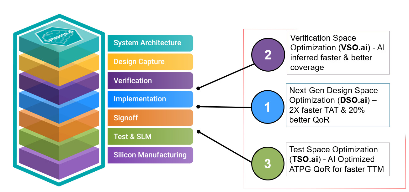
Synopsys is hosting a seminar series that explores how companies can leverage AI-driven EDA technology to deliver significant quality of results and productivity improvements across the development flow. The series will discuss how Synopsys.ai™, the industry’s first full-stack, AI-driven EDA suite, can help tackle the PPA (power, performance, and area), verification, and test challenges associated with today’s complex designs.
The first presentation of this three-part series targets design engineers looking to optimize PPA targets using Synopsys Design Space Optimization solution, DSO.ai™. The second webcast focuses on the verification engineer and how to achieve higher quality verification coverage faster with Synopsys Verification Space Optimization solution, VSO.ai™. The third webcast addresses the challenges faced by test engineers to reduce the number of test patterns while optimizing defect coverage with Synopsys Test Space Optimization solution, TSO.ai™. All three presentations will illustrate how to eliminate redundant and repetitive tasks using the respective sophisticated Synopsys.ai technology.
The future of innovation rests on the adoption of critical AI technologies. We can no longer burden ourselves with traditional manual tasks if we are to beat the competition. AI-driven EDA technology will allow companies to focus on chip quality and differentiation and empowers engineers to get the right chip with the right specs to market faster.
Register for the Synopsys.ai webinar series today!
Also Read:
Is Your RTL and Netlist Ready for DFT?
Synopsys Expands Agreement with Samsung Foundry to Increase IP Footprint
Requirements for Multi-Die System Success
Share this post via:


Comments
There are no comments yet.
You must register or log in to view/post comments.