
The increasing demands for massive amounts of data are driving high-performance computing (HPC) to advance the pace in the High-speed Ethernet world. This in turn, is increasing the levels of complexity when designing networking SoCs like switches, retimers, and pluggable modules. This growth is accelerating the need for the bandwidth hungry applications to transition from 400G to 800G and eventually to 1.6T Ethernet. In terms of SerDes data-rate, this translates to 56G to 112G to 224G per lane.
The Move from NRZ to PAM4 SerDes and the Importance of Digital Signal Processing Techniques
Before 56G SerDes, Non-Return-to-Zero (NRZ) signaling was prevalent. It encoded binary data as a series of high and low voltage levels, with no returning to zero voltage level in between. NRZ signaling is mostly implemented using analog circuitry since the processing latency is low, which is suitable for high-speed applications. However, as the data rates increased, the need for more advanced signal processing capabilities emerged. Digital circuits became more prevalent in SerDes designs in 56G to 112G to 224G. Digital signal processing (DSP) circuits enabled advanced signal processing, such as equalization, clock and data recovery (CDR), and adaptive equalization, which are critical in achieving reliable high-speed data transmission.
Furthermore, the demands for lower power consumption and smaller form factor also drove the adoption of digital SerDes circuits. Digital circuits consume less power and can be implemented using smaller transistors, making them suitable for high-density integration. Pulse Amplitude Modulation with four levels (PAM4) has become a popular signaling method for high-speed communication systems due to its ability to transmit more data per symbol and its higher energy efficiency. However, PAM4 signaling requires more complex signal processing techniques to mitigate the effects of signal degradation and noise, so that the transmitted signal is recovered reliably at the receiver end. In this article, we will discuss the various DSP techniques used in PAM4 SerDes.
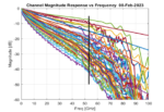
Figure 1: PAM4 DSP for 112G and beyond
DSP techniques used in PAM4 SerDes
Equalization
Equalization is an essential function of the PAM4 SerDes DSP circuit. The equalization circuitry compensates for the signal degradation caused by channel impairments such as attenuation, dispersion, and crosstalk. PAM4 equalization can be implemented using various techniques such as:
- Feedforward Equalization (FFE)
- Decision-Feedback Equalization (DFE)
- Adaptive Equalization
Feedforward Equalization (FFE) is a type of equalization that compensates for the signal degradation by amplifying or attenuating specific frequency components of the signal. FFE is implemented using a linear filter, which boosts or attenuates the high-frequency components of the signal. The FFE circuit uses an equalizer tap to adjust the filter coefficients. The number of taps determines the filter’s complexity and its ability to compensate for the channel impairments. FFE can compensate for channel impairments such as attenuation, dispersion, and crosstalk but is not effective in mitigating inter-symbol interference (ISI).
Decision-Feedback Equalization (DFE) is a more advanced form of equalization that compensates for the signal degradation caused by ISI. ISI is a phenomenon in which the signal’s energy from previous symbols interferes with the current symbol, causing distortion. DFE works by subtracting the estimated signal from the received signal to cancel out the ISI. The DFE circuit uses both feedforward and feedback taps to estimate and cancel out the ISI. The feedback taps compensate for the distortion caused by the previous symbol, and the feedforward taps compensate for the distortion caused by the current symbol. DFE can effectively mitigate ISI but requires more complex circuitry compared to FFE.
Adaptive Equalization is a technique that automatically adjusts the equalization coefficients based on the characteristics of the channel. It uses an adaptive algorithm that estimates the channel characteristics and updates the equalization coefficients to optimize the signal quality. The Adaptive Equalization circuit uses a training sequence to estimate the channel response and adjust the equalizer coefficients. Circuit can adapt to changing channel conditions and is effective in mitigating various channel impairments.
Clock and Data Recovery (CDR)
Clock and Data Recovery (CDR) is another essential function of the PAM4 SerDes DSP circuit. The CDR circuitry extracts the clock signal from the incoming data stream, which is used to synchronize the data at the receiver end. The clock extraction process is challenging in PAM4 because the signal has more transitions, making it difficult to distinguish the clock from the data. Various techniques such as Phase-Locked Loop (PLL) and Delay-Locked Loop (DLL) can be used for PAM4 CDR.
PLL is a technique that locks the oscillator frequency to the incoming signal’s frequency. The PLL measures the phase difference between the incoming signal and the oscillator and adjusts the oscillator frequency to match the incoming signal’s frequency. The PLL circuit uses a Voltage-Controlled Oscillator (VCO) and a Phase Frequency Detector (PFD) to generate the clock signal. PLL-based CDR is commonly used in PAM4 SerDes because it is more robust to noise and has better jitter performance compared to DLL-based CDR. DLL is a technique that measures the time difference between the incoming signal and the reference signal and adjusts the phase of the incoming signal to align with the reference signal. The DLL circuit uses a delay line and a Phase Detector (PD) to generate the clock signal. DLL-based CDR is less common in PAM4 SerDes because it is more susceptible to noise and has worse jitter performance compared to PLL-based CDR.
Advanced DSP techniques
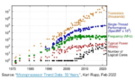
Maximum Likelihood Sequence Detection (MLSD) are used to improve the signal quality and mitigate channel impairments in high-speed communication systems requiring very long reaches. MLSD is a digital signal processing technique that uses statistical models and probability theory to estimate the transmitted data sequence from the received signal. MLSD works by generating all possible data sequences and comparing them with the received signal to find the most likely transmitted sequence. The MLSD algorithm uses the statistical properties of the signal and channel to calculate the likelihood of each possible data sequence, and the sequence with the highest likelihood is selected as the estimated transmitted data sequence. It is also a complex and computationally intensive technique, requiring significant processing power and memory. However, MLSD can provide significant improvements in signal quality and transmission performance, especially in channels with high noise, interference, and dispersion.
Figure 2: Need for MLSD: Channel Library of 40+ dB IL equalized by 224G SerDes
There are several variants of MLSD, including:
- Viterbi Algorithm
- Decision Feedback Sequence Estimation (DFSE)
- Soft-Output MLSD
The Viterbi Algorithm is a popular MLSD algorithm that uses a trellis diagram to generate all possible data sequences and find the most likely sequence. The Viterbi Algorithm can provide excellent performance in channels with moderate noise and ISI, but it may suffer from error propagation in severe channel conditions.
DFSE is another MLSD algorithm that uses feedback from the decision output to improve the sequence estimation accuracy. DFSE can provide better performance than Viterbi Algorithm in channels with high ISI and crosstalk, but it requires more complex circuitry and higher processing power.
Soft-Output MLSD is a variant of MLSD that provides probabilistic estimates of the transmitted data sequence. It can provide significant improvements in the error-correction performance of the system, especially when combined with FEC techniques such as LDPC. Soft-Output MLSD requires additional circuitry to generate the soft decisions, but it can provide significant benefits in terms of signal quality and error-correction capabilities.
Forward Error Correction Techniques
In addition to DSP methods, Forward Error Correction (FEC) techniques adds redundant data to the transmitted signal to detect and correct errors at the receiver end. FEC is an effective technique to improve the signal quality and ensure reliable transmission. There are various FEC techniques that can be used, including Reed-Solomon (RS) and Low-Density Parity-Check (LDPC).
RS is a block code FEC technique that adds redundant data to the transmitted signal to detect and correct errors. RS is a widely used FEC technique in PAM4 SerDes because it is simple, efficient, and has good error-correction capabilities. LDPC is a more advanced FEC technique that uses a sparse parity-check matrix.
Defining the Future of 224G SerDes Architecture
In summary, the IEEE 802.3df working group and the Optical Internetworking Form (OIF) consortium are focused on the definition of the 224G interface. The analog front-end bandwidth has increased by 2X for PAM4 or by 1.5X for PAM6 to achieve 224G. ADC with improved accuracy and reduced noise is required. Stronger equalization is needed to compensate for the additional loss due to higher Nyquist frequency, with more taps in the FFE and DFE. MLSD advanced DSP will provide significant improvements in signal quality and transmission performance at 224G. MLSD algorithms such as Viterbi Algorithm, DFSE, and Soft-Output MLSD can be used to improve the sequence estimation accuracy and mitigate channel impairments such as noise, interference, and dispersion. However, MLSD algorithms are computationally intensive and require significant processing power and memory, should carefully trade-off between C2M and cabled host applications.
Synopsys has been a developer of SerDes IP for many generations, playing an integral role in defining PAM4 solution with DSP at 224G. Now, Synopsys has a silicon-proven 224G Ethernet solution that customers can reference to achieve their own silicon success. Synopsys provides integration-friendly deliverables for 224G Ethernet PHY, PCS, and MAC with expert-level support which can make customers’ life easier by reducing the overall design cycle and helping them bring their products to market faster.
Also Read:
Full-Stack, AI-driven EDA Suite for Chipmakers
Power Delivery Network Analysis in DRAM Design
Intel Keynote on Formal a Mind-Stretcher
Multi-Die Systems Key to Next Wave of Systems Innovations


