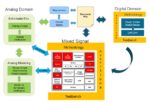
I have historically avoided mixed signal topics, assuming they decouple from digital and can be left to the experts. That simple view no longer holds water. Analog and digital are becoming more closely linked through control loops and datapaths, requiring a careful balancing act in verification between performance, accuracy and overall metric driven verification.
Improvements in support for this area are not a nice-to-have. A 2020 Wilson survey reported a significant jump in respins attributed to analog problems. Worse yet, system customers are now demanding unified metric data for coverage, safety, and power. We’ll need to jump out of our digital comfort zone to better understand full system verification challenges and solutions. My thanks to Shekar Chetput (R&D Group Director in Xcelium/Mixed Signal) and Paul Graykowski (Director Product Marketing), both at Cadence, for guiding me along this path. 😊
Application drivers and the mixed signal challenge
Sensors of all types require digital support to gather calibration and drift compensation data. Calibration is also a factor for IO interfaces; DDR provides a familiar example. RF for 5G/6G must support multiple bands and hybrid beamforming, again administered from the digital domain. Battery management systems, essential for EVs, handle sophisticated charging and usage behaviors such as preconditioning, fast charge, top-off and battery protection, all (you guessed it) overseen digitally.
Medical implants, held to very high standards of safety and reliability, now offer wireless communication, also sensing and actuators must be verified against body models (RC networks). Non-volatile memory cells handle multiple voltages and support circuitry for read, programming and wear/error detection. Even digital design depends on power management ICs (PMICs) supplying multiple voltages under digital control, supervising complex power management scenarios. These now extend to high voltage management in EVs.
Common to all objectives is the need to find a balance between the analog/RF world, where SPICE models are high accuracy but very low cycles/second, and the digital world with very high cycles/second throughput but very low analog accuracy (0/1 for voltage and no concept of current or impedance). Co-simulation is the obvious answer, but you can’t just bolt together low accuracy/high performance and high accuracy/low performance. These need intelligent interfaces.
Finding the right balance
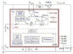
First make SPICE run faster and make digital simulation more accurate. Cadence speeds up SPICE through the Spectre FX simulator, for which portions of the circuit can run in any of 4 modes, from full analog accuracy to progressively abstracted modes preserving some level of accuracy while compromising complete precision.
To improve accuracy in digital a first step is Verilog-AMS/SystemVerilog wreal support, a real number signal good enough for simple interfaces. Something closer to analog modeling is possible through real number models (RNM) supported by Verilog/SV nettype, where a signal is modeled as a voltage, current and impedance structure, allowing for resolution between connected nets. Cadence provides an RNM nettype EEnet (Electrically Equivalent net). With EEnets it is possible to build a meaningful behavioral model running tests orders of magnitude faster while able to approach SPICE-level accuracy in some use-cases.
Together Spectre FX and RNM/EEnet models provide a spectrum of possibilities for modeling. A full behavioral wreal or EEnet model can be very useful in architectural design to explore different options without getting too bogged down in detail. When models are available, Shekar tells me this use case is now attracting a lot of attention.
In more detailed verification mix and match is often ideal: RNM for certain analog blocks for speed, and SPICE level where accuracy is important, such as in sensitivity analyses against supply voltage and temperature variations, beyond the scope of RNM analyses.
Building models
This all sounds great, but where do these models come from? The basic nettype is flexible but very low-level requiring significant investment from an analog designer unfamiliar with SystemVerilog. Cadence has an EEnet standard library of common base circuits (think capacitors, diodes, inductors, MOS devices), also a test library of mixed signal modules showing examples of how these components are used. Designers can build more complex components schematically using these components.
Shekar tells me that working with customers from the very early days of EEnet this base library is very stable and has recently been released as a part of the Xcelium Mixed-Signal App. Cadence is now working on building and reviewing several mid-level components (think PLLs, voltage regulators, ADCs, DACs). Their customers are also building their own mid-level components, extending even further to more complex functions. It seems necessity is driving progress rather than waiting for pre-packaged libraries.
A quick digression on standardization since significant effort goes into building models. Lu Dai (Accellera chair) told me at DVCon this year that the Accellera mixed signal working group is very active, and that demand from users is intense. Cadence is a participant and has an established reputation in this domain, so I assume their releases are likely to be close to whatever is finally agreed in the standard. Lu warned however that some SV mixed signal update requests are moving slowly since the SV standard is now under IEEE where updates are infrequent. Accellera are considering workarounds.
Testbench automation, assertions, coverage, etc
Higher simulation throughput is always an important goal but mixed signal verification teams need more. They want the automation their digital peers routinely use and have been lobbying hard to get these extended to mixed signal. A UVM-AMS working group under Accellera is already underway to this end. A standard is not yet released and is also wrestling with scheduling problems, but they are on the right track.
In the meantime, designers and verifiers serve these needs through proprietary flows; I imagine these too are tracking the evolving standard. Cadence supports metric driven verification across digital and analog through UVM testbenches, regular assertions and complex mixed signal assertions, together with randomization. For pure analog, coverage and other status can be imported from the Virtuoso ADE Verifier into vManager.
In summary, there have been significant advances in mixed signal verification and there is hope for progress through standardization. Mixed-signal verification truly is becoming a first-class partner with digital verification. You can get more information about the Xcelium Mixed Signal app HERE, the Spectre FX simulator HERE and a useful webinar on mixed signal HERE.


