- What kind of recovery do we expect, if any, after 2 down years?
- What impact will China have on the recovery of mature market chips?
- What will memory recovery look like? Will we return to stupid spend?
- Stock selection ever more critical in tepid recovery
Chip stocks have rocketed but the industry itself, not so much, “Anticipation….is keeping me waiting”
You wouldn’t know that the semiconductor industry has been in the doldrums for two years and more from the look of semiconductor stocks but that’s the reality.
The stock market seems to always be a leading indicator of future performance but then again the stocks have been pricey all through the down cycle seemingly anticipating a recovery that was always delayed.
The question now at hand is if 2024 will finally be the recovery that everyone has been anticipating?
So far the signs look OK but certainly not what we would call great and in no way back to the very heady days of crazy spending and expectations.
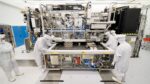
The very high spend that the industry saw to build capacity after the Covid induced shortage clearly overshot the runway by quite a bit which resulted in the overcapacity induced downcycle that has lasted over 2 years now.
We think chip makers will likely be a bit “gun shy” about spending capex given the length of the downturn.
We saw that TSMC is projecting “flattish” spend for 2024 and projects such as Arizona are pushed out or going slow on purpose.
TSMC not doing a buy High NA buy from ASML will also keep their capex under control.
Intel is spending at a reasonable clip but far from overspending, and appears to be more selective related to technology rather than capacity.
We certainly don’t expect Samsung to bounce back in memory spend as memory capacity is still off line and not fully back to 100% utilization. The primary spend we see out of Samsung is again technology driven not capacity driven
Technology spend without capacity spend is a muted up cycle
The semiconductor industry is importantly more than just a singular supply/demand capacity driven cycle.
The secondary cycle, though not as big as the capacity cycle, is the technology cycle. We obviously go through technology nodes and new fabs which create a separate wave of spend in parallel to the overall capacity driven spend.
We expect much of the spend in 2024 to be technology driven rather than capacity related and thus to be lower in amplitude.
Intel is spending on technology as is TSMC. Samsung and other memory makers have to keep up with technology node transitions even while keeping capacity off market. They need to keep up with technology to remain competitive on a Moore’s Law basis which drives basic costs in the memory business.
Essentially, technology spending remains almost a constant, though variable, while capacity spend has big swings.
We would temper expectations for a rip roaring Capacity spend in 2024
We don’t see a huge potential jump in demand for either memory or logic in 2024 that would bring back full fledged capacity spending.
While AI remains the near term focus and driver of the industry at the margin, AI alone is not enough to get the entire industry back in gear at full speed.
High bandwidth memory is great but far from enough to soak up all the excess memory capacity especially since retooling is needed to convert capacity to high bandwidth production. Memory makers are going to have to be careful not to overshoot HBM memory demand that may be more limited by AI logic chips capacity and availability.
We still need a more broad based macro-economic recovery to push demand for PCs, servers & wireless which are far and away the majority of the market.
The China Syndrome
It is still unclear what the impact of the $40B worth of semiconductor equipment tools bought by China in 2023 will have on the chip making market.
Obviously they are not all on line and productive, just yet. The question is, when they come on line what the impact will be?
There are already signs of weakening foundry pricing at the trailing edge where China plays as China wants to put equipment and all its new fabs to work and take market share.
$40B is an awful lot of equipment and likely doubly so as its not relatively expensive bleeding edge equipment which suggests that the $40B represents even a larger bump in capacity since its mostly at trailing edge.
It obviously does not include big ticket items like $150M EUV tools or even expensive DUV immersion tools.
So this is a very significant bump in capacity as it is all concentrated on lower cost, mature nodes.
Second tier foundries will get squeezed
We remain concerned that second tier foundries such as Global Foundries and UMC etc… will likely get squeezed between China catching up and cutting prices to gain market share at the low end and TSMC lowering pricing to keep market share. Both China and TSMC have significant cost advantages over mid range foundries.
The main way to avoid this will be to try to lock in business from customers who don’t want to do business with China for what ever reason. GloFo has done a good job of this but the vast majority of chip customers just care about price, price and delivery.
China will likely be on of the biggest factors keeping a lid on the rate of recovery in the semiconductor industry in 2024. While it has no impact on the leading edge , we need to remember that the vast majority of semiconductor units is for mature technologies that China already serves and can and will impact that large market.
We know what Chinese competition did to the LED and Solar panel markets.
Stock selectivity matters
We think there will be more differentiation in the performance of semiconductor companies going forward into 2024, so stock selection will matter more as not all stories will rise with the same tide.
We still like the ASML story. One of the few true tech monopolies in the market. The High NA roll out story that will present positive news flow which will overshadow and China restrictions.
We like TSMC as the main beneficiary of the AI revolution as well as near term demand from both Apple and Intel. They are cautiously spending and more immune from Chinese competition in the trailing edge. They are still the best chip maker in the world hands down.
Samsung is more of a mixed story as its foundry offerings still don’t fully measure up to anywhere near TSMC and memory will likely have a slow recovery as demand is still not huge. Pricing has moved off a long term bottom for memory but not a strong bounce just yet. It feels more like the restrictions in capacity finally had an impact rather than a return of strong demand. If this is correct and memory prices are better due to holding capacity off line its not going to be a super recovery.
Still HBM remains a bright spot although limited
We might be more inclined to look at SK Hynix as a pure memory play as opposed to Samsung which is under performing in foundry.
In general we would be more selective in purchases of stocks as many are already overbought and many of those are overbought for no good reason and could see weakness as reality of differentiation sets in.
The Stocks
We think overall this earnings season will be positive for chip stocks as we expect many management teams will talk about a brighter outlook for 2024 even though it remains more of a hope than reality.
The dream of AI is still one of the biggest drivers of the outlook for a recovery and so far AI hasn’t hit any major bumps that would see it slow down.
Equipment spending recovery will be slower as compared to chip producers as there is still not huge demand for capacity in either memory or general foundry (other than China spending)
There is still a very wild card of geo-politics and China/Taiwan. The pot of tensions continues to boil, perhaps on the back burner rather than the front burner as the rhetoric has been dialed down a notch or two. We haven’t heard a lot out of Gina Raimondo and there haven’t been any recent major military exercises.
The stocks still feel overbought as the S&P broke back into record territory. Perhaps its just P/E expansion as everyone likes to believe rather than over exuberance that investors fear.
I guess we will find out if earnings season can support the stocks resurgence.
About Semiconductor Advisors LLC
Semiconductor Advisors is an RIA (a Registered Investment Advisor),
specializing in technology companies with particular emphasis on semiconductor and semiconductor equipment companies. We have been covering the space longer and been involved with more transactions than any other financial professional in the space. We provide research, consulting and advisory services on strategic and financial matters to both industry participants as well as investors. We offer expert, intelligent, balanced research and advice. Our opinions are very direct and honest and offer an unbiased view as compared to other sources.
Also Read:
Is Intel cornering the market in ASML High NA tools? Not repeating EUV mistake
AMAT- Facing Criminal Charges for China Exports – Overshadows OK Quarter
The Coming China Chipocalypse – Trade Sanctions Backfire – Chips versus Equipment