Dieter Therssen obtained his master’s degree in Electronics Engineering from KU Leuven in 1987. He started his career as a hardware design engineer, using IMEC’s visionary tools and design methodologies in the early days of silicon integration.
Since then, Dieter developed his career across many digital technologies, in a broad range of applications and for a variety of companies. He’s been development manager of the International Technology Center Leuven; led the Audio Competence Center at Philips Semiconductors in Nijmegen; co-founded NXP software and Beatbrew; was Director for European automotive business at Premium Sound Solutions 2011, later transitioning its electronics business into Lear Corporation; and directed DSP Valley, an independent cluster of digital companies in the Low Countries.
Being CEO of Sigasi, a fast-growing, creative technology company in a B2B setting, is a perfect fit for Dieter. Having worked in that space for several companies, and well-rooted in the field of semiconductors, Dieter forever enjoys the magic of a motivated team.
Tell us about Sigasi.
Sigasi is redefining hardware description language (HDL) creation, integration, and validation in the digital design specification world. Our driving force is the shift-left principle: instilling the importance of catching potential errors and issues in specifications as early as possible in the design cycle.
HDL has long been created by talented designers writing code in simple environments, which they then need to slowly check manually, or rely on teams further down the line to point out errors. Sigasi is here to improve this onerous, laborious hardware design workflow. Why not create HDL specifications much more smoothly, integrate various time-saving methodologies and tools into the work, and validate code before it throws monkey wrenches into the simulation and synthesis flows, or the physical implementation flow? Sigasi makes all this possible.
In terms of the industry, Sigasi sits at the intersection of HDL creation and its hand-off to the down-stream EDA workflow. As a digital chip design verification company, we help hardware designers focus on their design content because our Integrated Design Environment (IDE) verifies their code as they’re typing or importing it.
What is the Shift-Left Methodology?
To understand Shift Left, it’s best to understand how hardware—and perhaps software designers—depict the flow of a design moving from a concept to a real chip. That starts at the left-hand side of the drawing board and ends up at the right-hand side.
On the right side, picture chips lying on a desk or sitting on a PCB and being tested. Think of architects that come up with how to solve this real-world problem in one way or another. Moving from one side to the other, hardware designs go through a lot of steps, a lot of transformations. Fixing a problem as it occurs later in the chain costs outrageously more than fixing it at the start of the process.
Harry Foster at Siemens has shown how costly mistakes can be in the chip design flow.
It’s shocking to see that the magnitude of cost involved on the left-hand side of the picture, as opposed to the right-hand side, is a factor of 40,000. That’s the magnitude of cost involved in undoing errors. Catch them at the beginning and pay 40,000 times less than if they are caught at the end.
Essentially, we’re talking about the principle that catching errors much earlier in the design can save a lot of money, certainly when compared to catching them towards the end of the design. Shifting left prevents costly mistakes and makes hardware design more efficient from the start.
What problems is Sigasi solving?
For more than 60 years, we have seen semiconductor manufacturers going to smaller nodes, bigger wafers, stretching lithography to the EUV spectrum, deploying more efficient materials, and even changing the implementation of the transistor, with FinFET and GAA as the latest incarnations. As a result, those manufacturers are offering enough real estate to put 200-billion transistors on a chip.
What is often forgotten is that designs still need to be created with that same capacity. That is the EDA world. Designers ultimately create layout files that manufacturers use to start their implementation process. The transformation of the layout files into lithography masks is after all the first step in the manufacturing process. Therefore, tools leading to the creation of those layout files also need to keep changing to keep up with capacity and the ever-changing physical manifestations that impact performance, power, and area (PPA). And that starts with the specification of an FPGA, ASIC, or SoC application.
What application areas are Sigasi’s strongest?
Any market that efficiently deploys artificial intelligence (AI) introduces complexity and uncertainty into the front-end design flow. Advantages of AI in the medical world result in better ways to perform and analyze MRIs, CTs, X-rays, EKGs, and other tests. This opens the door for new, AI-deploying chip designs. Sigasi offers the guardrails needed to resolve the uncertainty of AI creativity, with a deterministic validation flow.
The Race for Space is creating competition for exploration, homeland security, communication, and such is leading to opportunities worldwide to create satellites filled with AI-powered ICs. Design complexity is challenging. Another is the automotive sector where Advanced Driver-Assistance systems (ADAS) combined with sophisticated infotainment and hybrid engines has led to an explosion of Electronic Control Units (ECU) needed for cars. A hybrid SUV has more than 100 ECUs. This complexity goes beyond the cognitive abilities of most humans. Sigasi offers the organization that is now essential to designing the ICs for such complex systems.
Whether a company makes one or a million chips a year for space applications, they still need to be designed—free of errors.
What keeps Sigasi’s customers up at night?
HDL designers worry about complexity and the need to manage all the risks. Even an expert HDL coder can’t keep track of all the requirements for an appropriate coding style. Safety measures, security vulnerabilities, and PPA constraints impose rules and measures that need to be addressed in HDL ahead of hand off.
A designer’s nightmares are full of missed deadlines and schedule slips, cost overruns, falling short of goals, writing poor test benches, HDL design integrity so the specification must correspond to intent. Verification methodologies such as UVM ease writing good test benches, yet another worry added to the broad check-box list. Integrating HDL leads to mixing SystemVerilog and VHDL when the ideal library or IP might not be available in the preferred hardware design language.
The nightmare scenarios are endless.
What does the competitive landscape look like and how does Sigasi differentiate?
Many linting tools are commercially available. It takes time before they work their way through the design, compile it and come up with feedback for the user, which is typically verbose. They do a great job, of course, but they do catch errors on a delay. Designs need to be finished and free of syntax errors before you can run them.
Our differentiation is our shift-left approach. Our tools are upfront and real-time. We incrementally compile the entire design with every stroke of a keyboard, which is fundamentally different from what the other tools do.
Moreover, we are unique in how our solutions don’t just offer users an information dump, but rather give focused, relevant feedback. When building our tools, Sigasi engineers think about whether a problem could be the consequence of a preceding problem, and how it might be more efficient to report only the first problem, since fixing it will also fix the other problem. That is how we compile a succinct summary of what is wrong with the design. Our engine understands the semantics of SystemVerilog and VHDL. It is not just an editor or spell check. It understands how these languages work and what different combinations could mean—ensuring a hardware engineer gets fast, germane reporting.
What new features/technology is Sigasi working on?
We’re putting the finishing touches on an updated product portfolio and hierarchy of product offerings. Expanding our product lines will help individual designers verify their code and entire groups ensure their projects are on track and doing what they should do without constantly making changes.
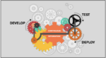
SemiWiki readers can expect more of the software world’s best practices in Sigasi’s products, going beyond our shift-left approach. For example, we’ll be introducing our command language interface (CLI), which is essential for the automation of any workflow. But it certainly comes in handy for continuous integration/continuous deployment (CI/CD)––a concept borrowed from the software world, where it’s customary for engineers to work in agile ways––that looks at the entire main code repository.
How do customers normally engage with Sigasi?
Our website is sigasi.com. Sigasi can be reached by e-mail at info@sigasi.com. We’re also on LinkedIn @company/sigasi/.
We’ll also be at DAC flying our new logo and tagline “Put Your Semicolons to Work” while exhibiting its Sigasi Visual HDL at DAC Booth #2416 (second floor).
Also Read:
CEO Interview: Barry Paterson of Agile Analog