What looks like a modest market expansion strategy is all but modest.
Insights into the Semiconductor Industry and the Semiconductor Supply Chain.
As usual, when TSMC reports, the Semiconductor industry gets a spray of insights that help understand what goes on in other areas of the industry. This time, TSMC gave more insight into their new Foundry 2.0 strategy, which will be covered later in this post.
The Q2-2024 result was a new revenue record indicating that the Semiconductor industry is out of the downcycle and ready to aim for new highs.
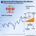
However, TSMC’s gross and operating profits have not returned to the same levels as last time, when revenue was over $20B/qtr. This is a new situation that needs to be uncovered.
Semiconductor manufacturing companies need to spend significant capital every quarter to maintain and service their equipment. Spending at the maintenance capex level ensures that manufacturing capacity does not decline.
From the end of 2020 until the end of 2023, TSMC made a significant capex investment above maintenance. The company then dropped capex to just above maintenance. This capacity is now flowing online, which has lowered TSMC’s utilisation revenue. The TSMC of Q2-24 has a lot more capacity at the last peak.
TSMC’s management did report increasing manufacturing utilisation, which means there is still spare capacity, although it might not be the capacity that TSMC needs.
There were other levers of Gross margin revealed in the investor call.
While the increasing manufacturing activity combined with the payment of Subsidies and selective price increases lifted the gross margin, there were also headwinds.
Inflation is increasing the cost of materials. As Taiwan’s largest electricity consumer, TSMC depends on grid expansion to fuel future growth. The investment in new and cleaner electricity is increasing electricity prices.
Also, the higher operating costs of the future manufacturing facilities in Arizona and Kumamoto would negatively impact gross margins.
Lastly, the company mentioned the conversion from 5 nm to 2 nm. It was earlier indicated that this was only Apple, but now it looks like TSMC is under great pressure from more of its HPC customers to migrate to 2nm.
Migrating customers takes time and effort, and it also takes time before manufacturing is sufficiently stable to generate good yields and become economically viable.
The market view
Unsurprisingly, TSMC is increasingly becoming THE supplier to the high-performance computing industry, as seen in the Q2-24 share of divisional revenue. Mobile is still significant, mainly due to Apple, but it is decreasing in share.
A revenue timeline shows the growth in Q2-24 comes from a step function increase in HPC revenue.
The annual growth rate for High-Performance Computing has been impressive, but the quarterly growth rate is even higher. This represents 145% CAGR in HPC.
HPC’s revenue share is increasing relentlessly, and TSMC is becoming a high-performance computing company. This is one of the drivers towards TSMC’s new Foundry 2.0 strategy.
Technology
While Apple has made a long-term commitment to TSMC to obtain exclusivity to the new 2N process, this is not likely to last as long as Apple’s exclusivity to the 3nm process, which has lasted for a year.
TSMC expect the business transition to 2nm will be faster and involve more products than the transition to 3 and 5nm combined over the first two years.
This means more TSMC clients than just Apple (from 3nm) want to get to 2nm. Not surprisingly this will be Nvidia (from 4/5nm), AMD & Intel (from 5nm) as the main clients
It took the 3-5nm business four years to reach 50% of the total revenue, while it only took 3nm 2 quarters to get 15%.
A comparison between HPC and 3nm revenue shows a similar trajectory.
As Apple has been the only 3nm customer up until now, it would be natural to assume that the growth spike is due to Apple, but this is likely not the case.
Apple being a consumer oriented company has a very specific buying pattern due to the seasonality of its business.
While the Apple Cogs also represent mobile business and other, this pattern can be seen in the TSMC 3nm business also. Q3 and Q4 up and Q1 down.
You would expect the Apple 3nm business to go down in Q2 also. It likely did but TSMC’s 3nm business grew by 84% in Q2-24 so something else is going on.
The jump in revenue is likely to come from one of the 5nm customers of and as the 5nm revenue did not decline, it is a new product.
While it could be Nvidia, the AI giant is likely busy selling Blackwell products that is based on TSMC’s 5nm (4) process.
More likely this is Intel’s Lunar Lake or AMD’s Instinct series or an upgrade of the Zen 5. Both Intel and AMD is reporting soon and this article will be updated. From a strategic perspective, TSMC is moving from few customers using the leading edge technology to many. This also means TSMC is getting more important for its customers in High Performance Computing.
Technology Development
There is a good reason TSMC’s clients want to get to 2nm and even better technologies (N16). The performance gains are significant.
The relative performance improvements (in layman’s terms) can be seen below. Power Improvements (at similar speed) or Speed improvement (at similar power):
N16 is best used for specific HPC products with complex signal routes and dense power delivery and work. Volume production is scheduled for the second half of 2026
TSMC normally introduces intermediary upgrades for each of their processes and the benefits can be significant as seen in the N2P process. It is almost like an entire new process node but with less risk and cost. It will be incredibly attractive for the AI GPU combattants to get to these nodes as fast as possible. The balance of power is leaning more towards TSMC.
Cowos Capacity
From a strategic perspective, advanced packaging is becoming incredibly important and the main driver behind the Foundry 2.0 Strategy
Even though TSMC is adding as much advanced packaging technology as possible, it is nowhere near fulfilling the demand. TSMC expect to grow capacity by 60% CAGR but will not be able to meet demand before sometime during 2026 at best.
Margins have been low but are improving to a level close to corporate average margin as yields improve. CoWoS is the main reason that TSMC is changing its strategy to 2.0. All of the HPC customers will need advanced packaging to integrate High Bandwidth memory on an interposer. Later on this will be a need for PC processors and everything else AI.
The new 2.0 Foundry Strategy:
While the Foundry 2.0 strategy looks like a market expansion strategy from the $125B (2023) Foundry markets to add the packaging market of $135B bringing the total addressable market for TSMC to $250B. This changes TSMC’s market share from 55.3% to 28% in the new definition.
Apart from market expansion, Foundry 2.0 also aligns closely with the changed need of the top HPC customers, Apple, Nvidia, Intel, AMD and Broadcom. TMSC can basically deliver everything but the memory element of the CPU and GPU boards.
From a technology perspective, the move makes TSMC less dependent of the continuation of Moore’s law predicting continously smaller 2D geometries as the advanced packaging effectively opens up for 3D integration and technology advancement.
It represents the transformation of TSMC from a components company to a subsystems company, just like Nvidia’s transformation from GPU to AI Server boards.
As Nvidia developed Blackwell, it became obvious that the silicon for the GPU itself got diluted. The introduction of more memory, Silicon interposers and large slabs of advanced substrates, made the GPU share of the BOM decline. The Foundry 2.0 strategy is also aimed at controlling more of the supply chain in order to maintain TSMC’s importance as supplier to the CPU and GPU customers.
The capital allocation strategy, reveals the current fiscal importance of each of the main areas of TSMC business. If we didn’t know it, TSMC is still an advanced logic node company and that will continue. The new advance packaging, test and mass making (assembly??) will be allocated 10% of the total CapEx budget which is 31B$ in 2024.
While this sounds modest, the capital requirements for the Test and Packaging (OSAT) companies is a lot less than for semiconductor manufacturing. The largest OSAT companies are ASE and Amkor and they have CapEx spend of and estimated 2.5B$ in 2024. TSMC is dead serious about entering this industry and the established companies need to be on their toes.
Conclusion
TSMC’s new strategy has a title that completely lacks imagination but the strategy itself is very well developed and also very ambitious. While Intel and Samsung are busy figuring out how to get their advanced foundry nodes to work and finding customer for them, TSMC is expanding its silicon leadership into advanced packaging becoming a more important supplier to the key AI customers. This will also increase TSMC’s bargaining situation making the company able to command more of the value generation in AI if TSMC is not as modest and humble as normal.
Also Read:
TSMC Foundry 2.0 and Intel IDM 2.0
Q&A With TSMC on Next-Gen Foundry
Will Semiconductor earnings live up to the Investor hype?


