At the ISS Conference in January, An Steegen EVP of Semiconductor Technology & Systems at imec gave a talk entitled “Patterning Options for Advanced Technology Nodes”. I was present for her talk and had the opportunity to have a follow up interview with An.… Read More

Tag: imec
Fabless and IDMs Training up on Integrated Photonics
I had the good fortune to be able to attend a very informative five-day photonic integrated circuit (PIC) training this last week in Santa Clara, CA. The training was organized by Erik Pennings of 7 Pennies consulting and hosted by Tektronix. Several ecosystem partners from the design automation, photonic foundries and photonic… Read More
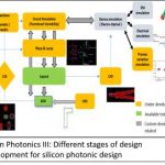
Making photonic design more straightforward

The arrival of optical computing has been predicted every year for the last fifteen years. As with any other technology backed by prolific research, lofty goals get dialed back as problems are identified. What emerges first is a set of use cases where the technology fits with practical, realizable implementations.
When it comes… Read More
IMEC Technology Forum at SEMICON – Coventor could save you billions!

The development of leading edge semiconductor technology is incredibly expensive, with estimates ranging from a few to several billion dollars for new nodes. The time to develop a leading edge process is also a critical competitive issue with some of the largest opportunities awarded based on who is first to yield on a new node.… Read More
IMEC-Horizontal Nanowires for 5nm at the VLSI Technology Symposium
At the VLSI Technology Symposium, IMEC presented a paper entitled “Gate-All-Around MOSFETs based on Vertically Stacked Horizontal Si Nanowires in a Replacement Metal Gate Process on Bulk Silicon Wafers”. I have wanted to blog about this paper since the symposium was held but also wanted to tie it in with an interview… Read More
Electrical-Optical Design, A Bridge to Terabitsia
If you don’t get the tongue in cheek reference of the title, you probably don’t have children who liked to watch Disney movies. All four of my daughters loved Disney and so, I am forever shaped by the Wonderful World of Disney. In 2007 Disney adapted to the screen a novel called, ‘A Bridge to Terabithia’, in which two adolescents escape… Read More
SEMICON West 2016 Preview
Next week is SEMICON West and I plan to be there all week. SEMICON West is a great opportunity to see the latest in equipment and materials on the show floor, to attend all the talks and receptions and to meet with various industry experts.… Read More
IMEC Technology Forum (ITF) – Secrets of Semiconductor Scaling
IMEC is a technology research center located in Belgium that is one of the premier semiconductor research centers in the world today. The IMEC Technology Forum (ITF) is a two-day event attended by approximately 1,000 people to showcase the work done by IMEC and their partners.… Read More
IMEC Technology Forum (ITF) – Moving the Electronics Industry Forward
IMEC is a technology research center located in Belgium that is one of the premier semiconductor research centers in the world today. The IMEC Technology Forum (ITF) is a two-day event attended by approximately 1,000 people to showcase the work done by IMEC and their partners.
Gary Patton is the Chief Technical Officer and Senior… Read More
IMEC Technology Forum (ITF) – EUV When, Not If
For me personally EUV has been something of a roller coaster ride over the last several years. I started out a strong believer in EUV but then at the SPIE Advanced Lithography Conference in 2014 TSMC gave a very negative assessment of EUV, and there was a SEMATECH paper on high NA EUV that struck me as extremely unlikely to succeed. I … Read More