You are currently viewing SemiWiki as a guest which gives you limited access to the site. To view blog comments and experience other SemiWiki features you must be a registered member. Registration is fast, simple, and absolutely free so please,
join our community today!
At SEMICON West I attended the imec technology forum, multiple Tech Spot presentations and conducted a number of interviews relevant to advanced lithography and EUV. In this article I will summarize what I learned plus make some comments on the outlook for EUV.… Read More
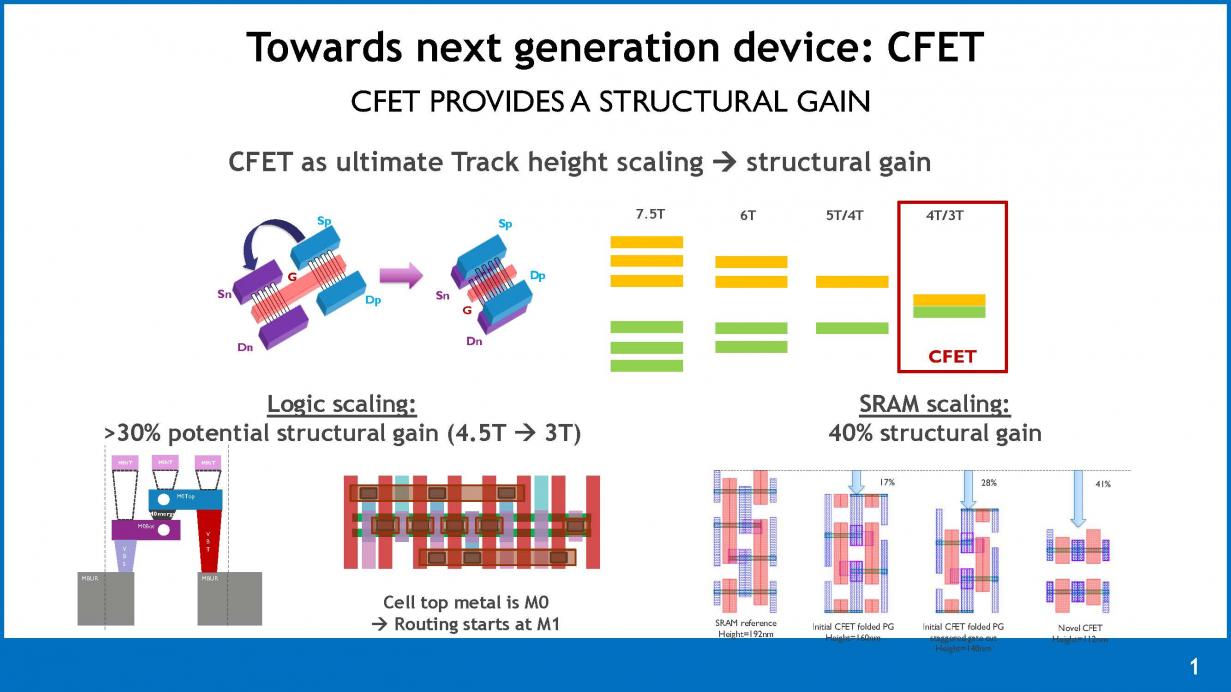
The 2018 VLSI Technology conference was held in Hawaii in June and is one of the premier conferences covering integrated circuit process technology and circuit design. The Complementary FET (CFET) is an emerging option to continue logic scaling into the next decade. At the conference imec, GLOBALFOUNDRIES, Tokyo Electron and… Read More
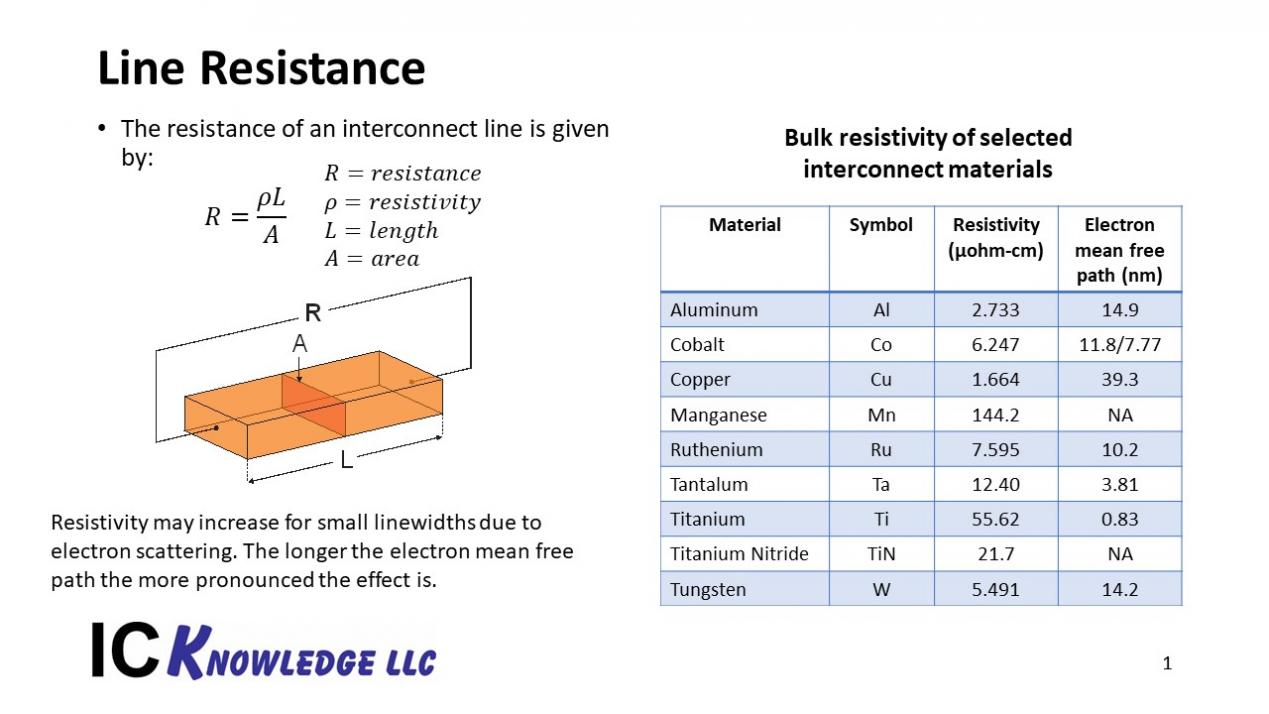
The IEEE Interconnect Technology Conference (IITC): Advanced Metallization Conference was held June 4th through 7th in Santa Clara. Imec presented multiple papers on comparing copper, cobalt and ruthenium interconnect. One paper in particular caught my eye: Marleen H. van der Veen, # N. Heylen, O. Varela Pedreira, S. Decoster,… Read More
At the Imec technology forum in Belgium, Dan Mocuta and Juliana Radu presented “Evolution and Disruption: A Perspective on Logic Scaling and Beyond”, I also had a chance to sit down with Dan and discuss the presentation.
Device scaling
Scaling of devices will only get you so far, you need to look at new devices and new… Read More
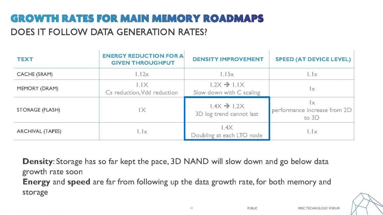
At the Imec technology forum in Belgium Gouri Sankar Kar and Arnaud Furnemont presented memory and storage perspectives and I also got to interview Arnaud. Arnaud leads overall memory development at Imec and personally leads NAND and DNA research.
Memory research is focused on power, energy, speed and cost with energy and throughput… Read More
One of the more frequent questions I get, “What is next after FinFETs?” is finally getting answered. Thankfully I am surrounded by experts in the process technology field including Scotten Jones of IC Knowledge. I am also surrounded by design enablement experts so I really am the man in the middle which brings us to a discussion between… Read More
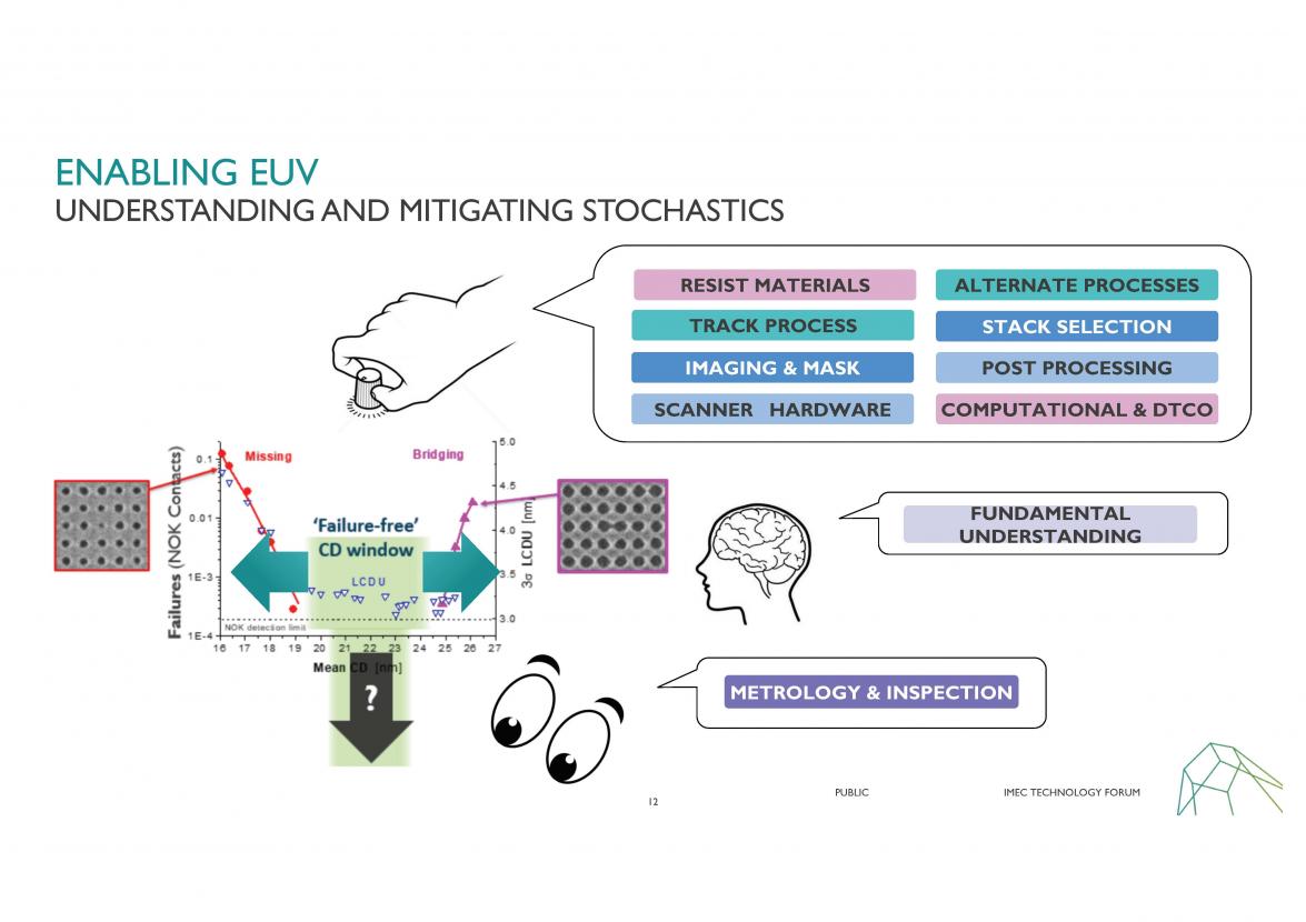
This year the Advanced Lithography Conference felt very different to me than the last couple of years. I think it was Chris Mack who proclaimed it the year of Stochastics. EUV has dominated the conference for the last several years but in the past the conversation has been mostly centered on the systems, system power and uptime.
I … Read More
At the IEDM 2017, imec held an imec technology forum and presented several papers, I also had the opportunity to interview Anda Mocuta director of technology solutions and enablement. In this article I will summarize the keys points of what I learned about the future of logic. I will follow this up with a later article covering memory.… Read More
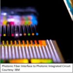
On September 6, 2017, Cadence Design Systems, Lumerical Solutions and PhoeniX Software hosted their second Photonics Summit. As with last year’s summit, this was a two-day event, with the first day including in a myriad of photonics presentations and the second day being a hands-on workshop. The hands-on workshop taught attendees… Read More
At SEMICON West I attended the imec technology forum where Zsolt Tokei presented “How to Solve the BEOL RC Dilemma” and the SEMICON Economics of Density Scaling session where Larry Clevenger of IBM presented “Interconnect Scaling Strategic for Advanced Semiconductor Nodes”. I also had the opportunity… Read More