You are currently viewing SemiWiki as a guest which gives you limited access to the site. To view blog comments and experience other SemiWiki features you must be a registered member. Registration is fast, simple, and absolutely free so please,
join our community today!
While there is a lot of excitement around the semiconductor shortage narrative and the fabs all being full, both 200mm and 300mm, there is one big plot hole and that is the FinFET era.
Intel ushered in the FinFET era only to lose FinFET dominance to the foundries shortly thereafter. In 2009 Intel brought out a 22nm FinFET wafer at the… Read More
I was asked to give a talk at the 2021 ISS conference and the following is a write up of the talk.
The title of the talk is “Logic Leadership in the PPAC era”.
The talk is broken up into three main sections:
- Background information explaining PPAC and Standard Cells.
- A node-by-node comparisons of companies running leading edge logic
…
Read More
The industry recently concluded a series of technology events for the all the major foundries. Done as virtual events this year, each one provided a significant update on technology platforms, roadmaps and ecosystem partnerships. These events are quite valuable to chip design teams who need to be aware of the latest in process,… Read More
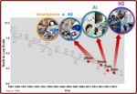
At the recent TSMC OIP Ecosystem Forum and Technology virtual events, TSMC re-affirmed their previous prediction that 5G is going to be a multi-year silicon mega-trend with the biggest drivers being the ramp up of 5G handsets, supporting infrastructure and the continued growth of high performance computing (HPC).
We all want… Read More
Summary
At the recent Intel Architecture Day 2020 symposium, a number of technology enhancements to the Intel 10nm process node were introduced. The cumulative effect of these enhancements would provide designs with a performance boost (at iso-power) approaching 20% – a significant intra-node enhancement, to be sure. The… Read More
I had the pleasure of spending time with Hiren Majmudar in preparation for the upcoming AI Accelerators webinar. As far as webinars go this will be one of the better ones we have done. Hiren has deep experience in both semiconductors and EDA during his lengthy career at Intel and now with a pure play foundry. He is intelligent, personable,… Read More
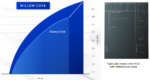
In this, the second part of a two-part series we delve further into defining worst case, this time focusing specifically on device performance.
In the last blog we talked about the steady increase in power density per unit silicon area and how worst case is definitely getting worse. We discussed how in each new FinFET node the dynamic… Read More
Summary
A recent process enhancement in advanced nodes is to support the fabrication of contacts directly on the active gate area of a device. At the recent VLSI 2020 Symposium, the critical advantages of this capability were highlighted, specifically in the context of the behavior of RF CMOS devices needed for 5G designs.
Introduction… Read More
Moore’s Law has been about device density, specifically transistor density, increasing every certain number of years. Although cost is the most easily grasped advantage, there are two other benefits: higher performance (speed) and reduced power. When these benefits are compromised, they can also pose a scaling limitation.
…
Read More
As transistor dimensions shrink to follow Moore’s Law, the functionality of the gate used to switch on or off the current is actually being degraded by the short channel effect (SCE) [1-5]. Moreover, the simultaneous reduction of voltage aggravates the degradation, as will be discussed below.
A Practical Lower Limit of… Read More