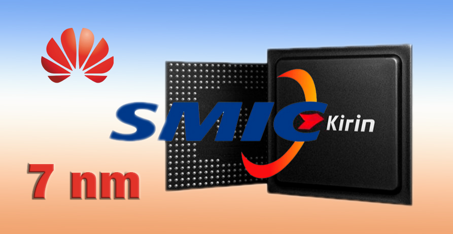
Recently TechInsights analyzed a Bitcoin Miner chip fabbed at SMIC and declared SMIC has a 7nm process. There has been some debate as to whether the SMIC process is really 7nm and what it means if it is 7nm. I wanted to discuss the case for and against the process being 7nm, and what I think it means.
First off, I want to say I am not going to reveal all the specific pitches, if you want that data you need to purchase a report from TechInsights.
Is it 7nm?
The key pitches for a process technology are Fin Pitch (FP), Contacted Poly Pitch (CPP) and Metal 2 Pitch (M2P). The SMIC pitches for FP are larger than TSMC 10nm FP, and the CPP and M2P are the same as TSMC 10nm. So is this really a relaxed 10nm process, it is not that simple.
The SMIC process also has some Design Technology Co-Optimization (DTCO) features not seen at 10nm. Specifically, TSMC and Samsung 10nm have 8.25 and 8.75 track height respectively at 10nm, SMIC is 6 tracks something that Samsung didn’t do until 5nm and TSMC at 7nm. SMIC also has a Single Diffusion Break (SDB) something Samsung had at 10nm but went away from at 7nm and didn’t get back to until 5nm, and TSMC didn’t implement until their second generation 7nm process (7+).
The bottom line to me is the high-density logic cell density for SMIC is 89 million transistors per millimeter squared, this is very similar to Samsung and TSMC first generation 7nm processes. In my opinion this is a 7nm “class” process and appears to be an acceptable 7nm alternative.
How did SMIC get here
I have seen several comments that SMIC copied TSMC’s first generation 7nm process, and while they may have adopted elements of it, there are a lot of differences too, for example as noted above, all the pitches are relaxed to 10nm or greater dimensions and some of the DTCO features are more advanced than TSMC’s first generation 7nm.
TSMC’s first generation 7nm process was an all-optical process with no EUV layers and due to the US blocking EUV systems from shipping to China, SMIC is limited to an optical approach and this process has no EUV layers.
I find the large CPP dimension particularly interesting. CPP is the combination of gate length, contact width and gate to contact spacer thickness. Gate length is limited by leakage and device type, contact width is limited by a company’s ability to drive down specific contact resistance and therefore achieve an acceptable contact resistance, gate to contact spacer thickness is limited by the capacitance of the spacer material and the resulting gate to contact parasitic capacitance. The fact that the CPP is “10nm like” suggests SMIC is still struggling with these processes. It is common to increase CPP to improve performance and this suggests to me that to get to acceptable performance SMIC had to do that.
Where can SMIC go from here
Assuming EUV systems continue to not be available in China, this limits SMIC’s options for further improvements. It seems likely the US will continue to block EUV shipments to China and I don’t see China developing their own EUV system any time soon.
The most straight forward approach in my view is to reduce the pitches to match TSMC’s first generation 7nm optical process, this combined with the SDB, and 6-track cell would yield a second generation 7nm or even 6nm process. I believe SMIC should be able to achieve this given some time to further optimize the process steps, this could be a reasonable goal for SMIC for 2023. This would contrast with Samsung and TSMC that both have had 5nm in production since 2020 and are currently ramping 3nm, with 2nm in development.
The next obvious question is could SMIC get to 5nm. Without EUV going below 7nm requires increasingly complex multi-patterning with increasingly restrictive design rules and spiraling costs. It is theoretically possible to do 5nm all optical or even 3nm. Self-Aligned Quadruple Patterning with immersion lithography can produce a 20nm pitch small enough for any 3nm requirements but would require a lot of cut masks for Fin and metal patterning to get there.
Conclusion
SMIC appears to have a serviceable first generation 7nm process now with a reasonable prospect to get to second generation 7nm/6nm in the near futures. 5nm and 3nm while theoretically possible would be highly constrained and expensive process versions if pursued due to the lack of EUV.
Also Read:
SEMICON West 2022 and the Imec Roadmap
The Lost Opportunity for 450mm
Share this post via:


Captain America: Can Elon Musk Save America’s Chip Manufacturing Industry?