Intel and TSMC make up two of the three leading edge logic companies. At IEDM held in December 2022, Intel presented a paper on 2D Materials and TSMC presented 6 papers. Clearly 2D materials are of great interest at least to two of the three leading edge logic companies. Before diving into the papers, some background context is needed.
Logic Scaling
Logic designs are made up of standard cells, if you are going to scale logic to increase density, the standard cells must shrink.
The height of a standard cell is typically characterized as the Metal-2 Pitch (M2P) multiplied by the number of tracks. While this is a useful metric, it glosses over the fact that the cell height must also encompass the devices that make up the cell. Figure illustrates a 7.5-track standard cell and shows the M2P and tracks on the left of the cell and also to the right of the cell is a cross sectional view of the corresponding device structure.
The width of a standard cell is made up of some number of Contacted Poly Pitches (CPP) with the number depending on the cell type and how the diffusion breaks at the edges of the cell are handled. Once again, CPP is made up of a device structure that must shrink when CPP shrinks. Figure 1 illustrates CPP and at the bottom has a cross sectional view of the device structure.
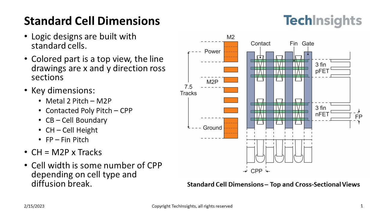
Figure 1. Standard Cell.
Intel, Samsung, and TSMC, have all made the switch from planar devices to FinFETs and are now at the beginning stages of the transition to Horizontal Nano-Sheets (HNS). Samsung is in production with HNS now, and Intel and TSMC have announced HNS production targets of 2024 and 2025 respectively.
Figure 2 illustrates the device structure and dimensions that make up cell height.
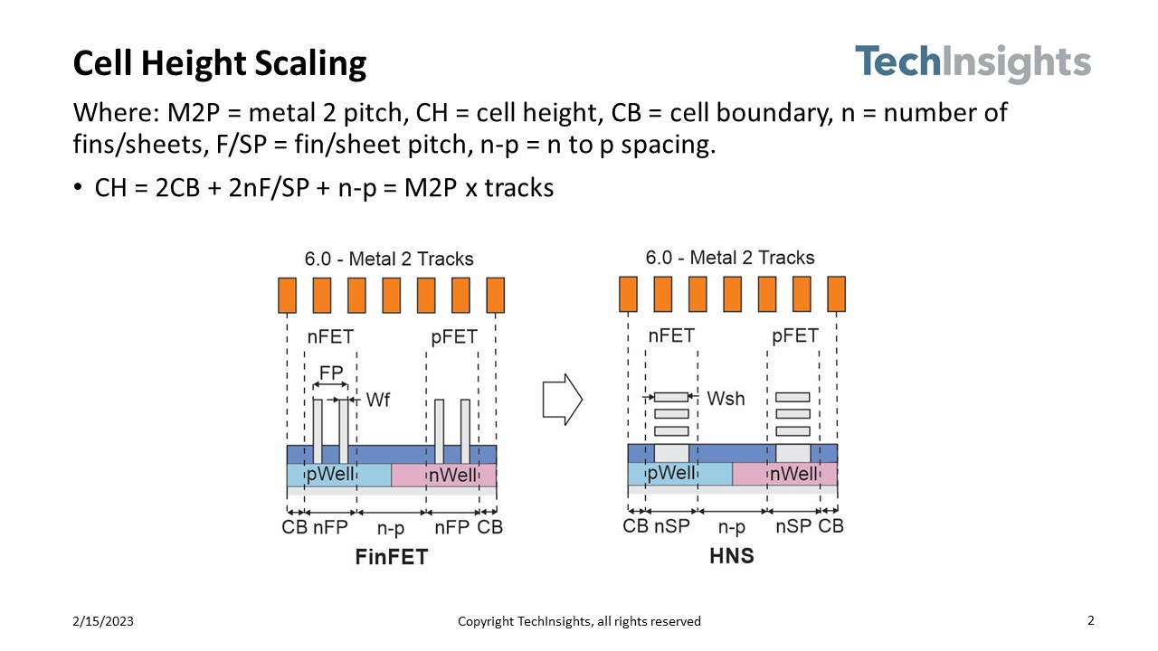
Figure 2. Standard Cell Height.
The change over to HNS offers multiple opportunities to shrink cell height. HNS can replace multiple fin nFET and pFET devices with single nano-sheet stacks shrinking the height impact of the devices. Forksheet and CFET enhancements to HNS can reduce or even eliminate n-p spacing.
CPP is made up of Gate Length (Lg), Spacer Thickness (Tsp) and Contact Width (Wc), see figure 3.
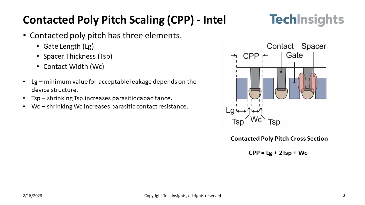
Figure 3. Contacted Poly Pitch.
CPP can be scaled down by reducing Lg, Tsp, or Wc or any combination of the three. Lg is limited by the devices ability to provide acceptable leakage. Figure 4 illustrates Lg length for various devices.
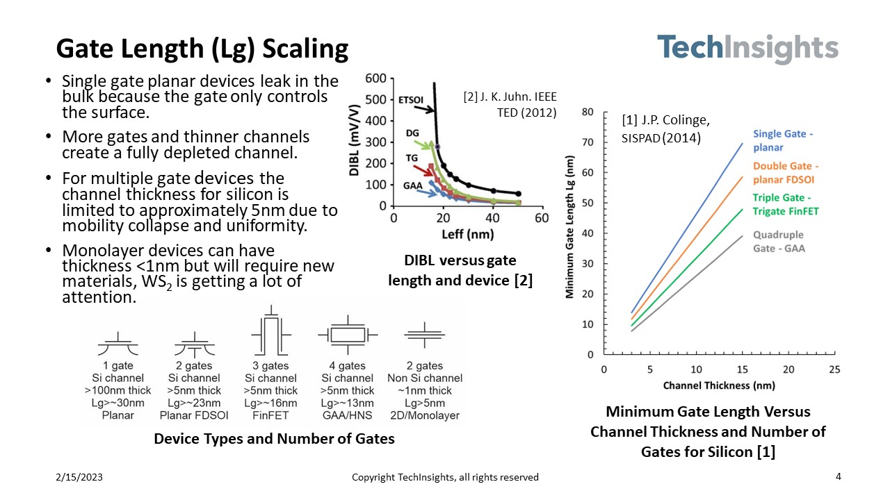
Figure 4. Gate Length Scaling.
From figure 4 constraining the channel thickness and/or increasing the number of gates enables shorter Lg.
So called 2D materials are made up of a monolayer of material less than 1nm thick improving gate control over the channel and enabling Lg down to ~5nm. At these dimensions silicon has poor mobility and other materials are used that have higher mobility and higher band gap further reducing leakage. The ability to scale Lg to ~5nm enables a significant shrink of CPP and therefore smaller standard cells.
2D Material Challenges
Transition Metal Dichalcogenides (TMD) such as MoS2, WS2, or WSe2, have been identified as materials of interest with high mobility at monolayer thicknesses (silicon has poor mobility at these dimensions). There are several challenges/questions that need to be addressed for practical use of these materials and they are explored in the 7 papers that will be discussed:
- Device performance – do devices fabricated with these materials really provide good drive current and low leakage at short Lg.
- Contacts – 2D TMD films are atomically smooth and hard to make good low resistance contact to.
- Film formation – currently MOCVD at high temperature on a sapphire substrate is used to form the 2D films and then the resulting film is transferred to a 300mm silicon wafer for further processing. This is not a practical production process.
Presented Results
In paper 7.5, “Gate length scaling beyond Si: Mono-layer 2D Channel FETs Robust to Short Channel Effects,” C. J. Dorow, et. Al., of Intel explored device performance.
The ultimate goal for 2D material based devices is a stack of 2D layers similar to the HNS stacks but with each channel being thinner enabling shorter Lg and more layers in a stack. Figure 5 illustrates the difference.
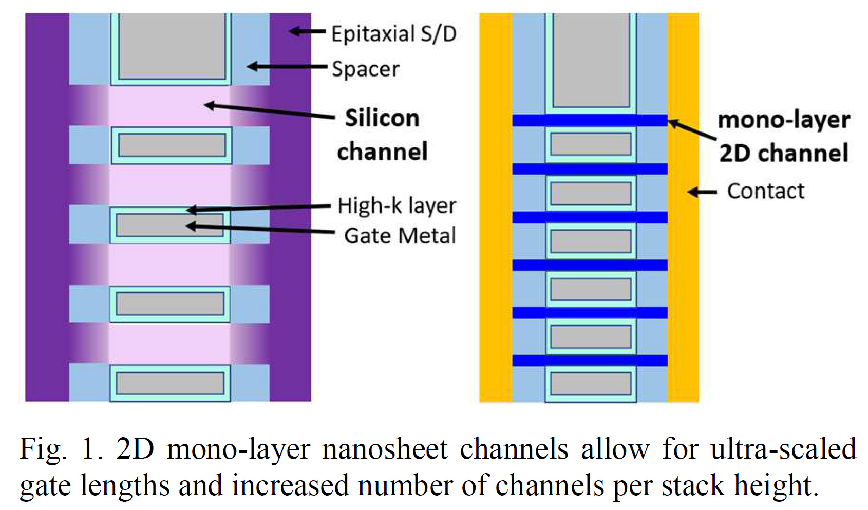
Figure 5. HNS Versus 2D Stack.
Intel did a wet transfer of an MBE grown MoS2 film over a back gate and then evaluated the device with a back gate and also with an added front gate down to a source-drain distance of 25nm. Figure 6 illustrates the device structure.
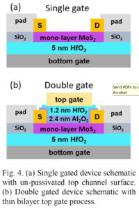
Figure 6. Intel 2D Device Structure.
Intel encountered some delamination issues in their experiments but were able to experimentally confirm their modeling result and conclude that a double gated device should be able to scale down to at least 10nm with low leakage, see figure 7.
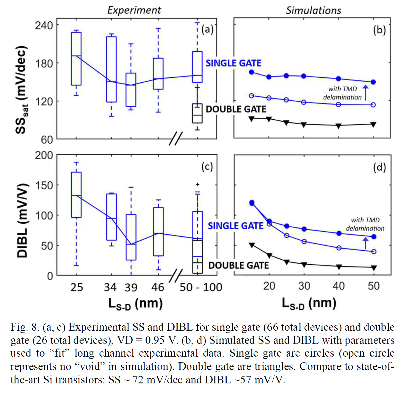
Figure 7. Experimental Results (left side) and Simulation Results (right side).
In paper 28.4, “Comprehensive Physics Based TCAD Model for 2D MX2 Channel Transistors,” D. Mahaveer Sathaiya, et. al., of TSMC, discussed a comprehensive simulation model of 2D devices and calibrated the model against 3 datasets. Having the ability to model 2D devices accurately will be key to the further development of the technology.
In paper 28.1, “Computational Screening and Multiscale Simulation of Barrier-Free Contacts for 2D Semiconductor pFETs,” Ning Yang, et. al., of TSMC, used ab initio calculations to screen contact materials for 2D devices.
The best reported experimental results for contact resistance to WSe2 are 950 Ω·μm and in this work Co3Sn2S2 is projected to be able to achieve 20 Ω·μm approaching the quantum limit. Furthermore, simulated devices are projected to produce ~2 mA/μm on state current. Sputtering on a sapphire substrate followed by a high-temperature annealing process (800 ̊C) was shown to produce Co3Sn2S2 with the expected chemical composition and crystalline structure.
In paper 7.2, “High-Performance Monolayer WSe2 p/n FETs via Antimony-Platinum Modulated Contact Technology towards 2D CMOS Electronics,” Ang-Sheng Chou, et. al., of TSMC, presented experimental results for Sb-Pt modulated contacts that achieve record contact resistance of 750 Ω·μm for pFET and 1,800 Ω·μm for nFET on WSe2. An on current of ~150 μA/μm was achieved. These results are not as good as the projections from paper 28.1 but represent experimental results versus simulations.
In paper 7.3, “pMOSFET with CVD-grown 2D semiconductor channel enabled by ultra-thin and fab-compatible spacer doping,” Terry Y.T. Hung, et. al, of TSMC, work towards a production type of pFET is presented. A lot of 2D material work is done on Schottky diodes but MOSFETs have lower access resistance. In order to create practical MOSFETs a CVD grown channel is needed with doped spacers. In this paper broken bandgap doped spacers are created by treating WSe2 with O2 plasma to create WOx as a dopant. The process is self-aligned and self-limiting as illustrated in figure 8.
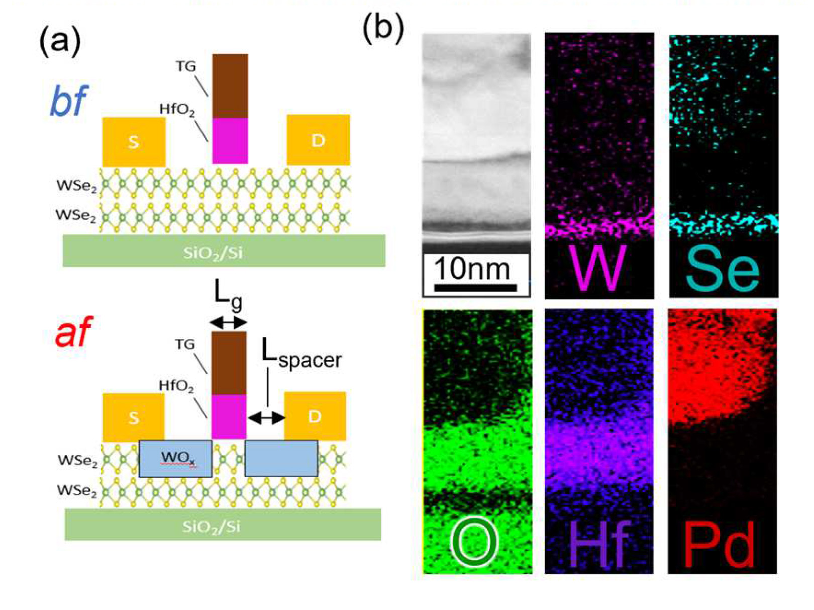
Figure 8. Self-aligned and Self-limited doped spacer formation.
The CVD grown 2D layers are still grown separately and then transferred but other parts of the process are production compatible. The devices achieved one of the lowest Rc ~ 1,000 Ω·μm among
transistors with WSe2 channel and relatively high Ion > 10-5 A/μm for a good S.S. < 80mV/dec.
In paper 7.4, “Nearly Ideal Subthreshold Swing in Monolayer MoS2 Top-Gate nFETs with Scaled EOT of 1 nm,” Tsung-En Lee, et. al., of TSMC showed an ALD grown Hf-based gate oxide of ~1nm EOT on CVD grown MoS2 with a top gate and achieve low leakage and a nearly ideal subthreshold swing of 68 MV/dec. Pinhole free oxide on TMD materials are very difficult to achieve and this work showed excellent results.
The final paper is 34.5, “First Demonstration of GAA Monolayer-MoS2 Nanosheet nFET with 410 μA/μm ID at 1V VD at 40nm gate length,” Yun-Yan Chung, et. al. of TSMC showed an MoS2 device with good performance fabricated with an integrated process flow.
Figure 9. illustrates a simulation of the process flow for a two-layer device stack.
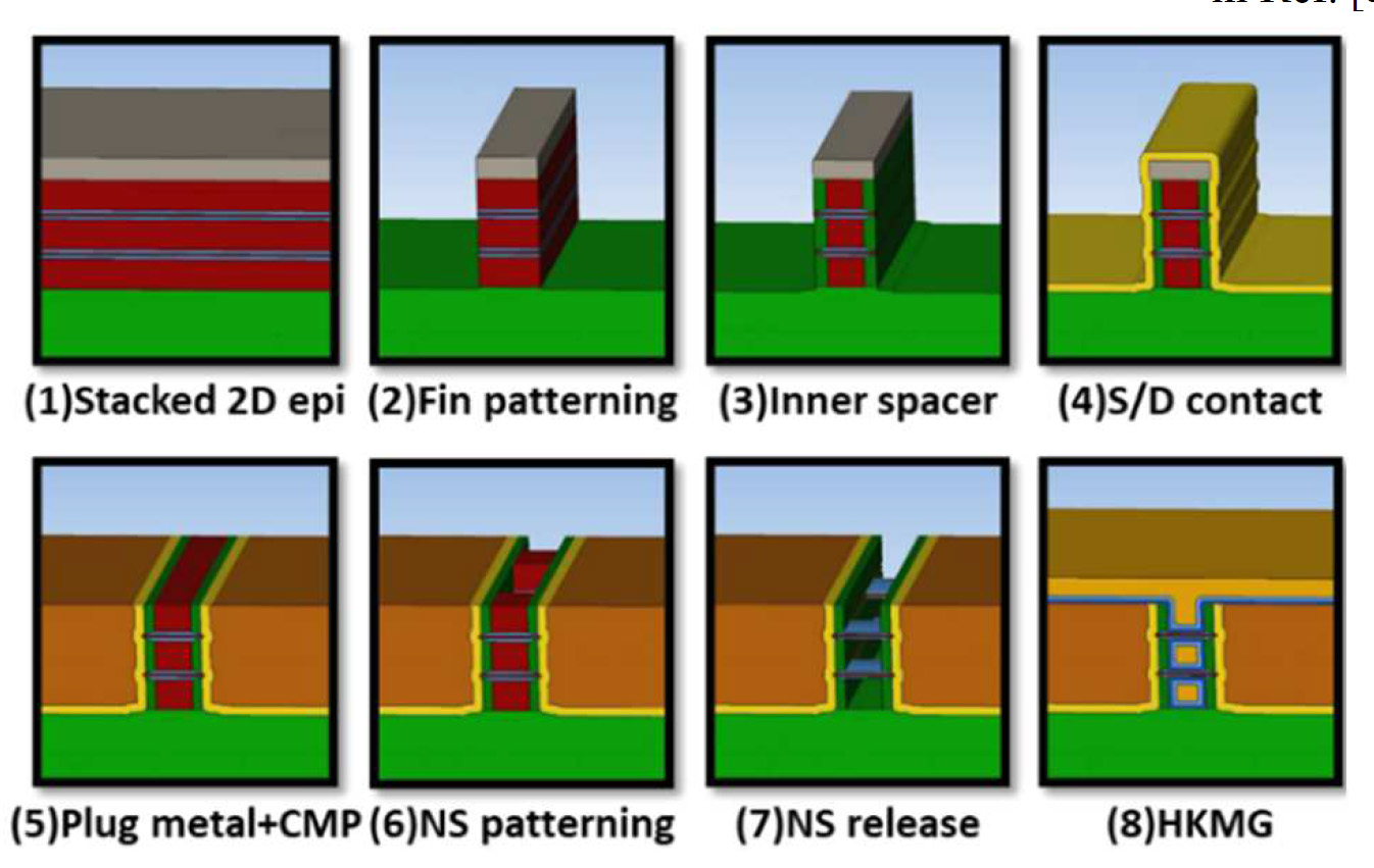
Figure 9. Simulated two layer device process.
Although further research is still needed in this paper 2 and 4 stacks of TMD and sacrificial material were sequentially deposited.
Figure 10. shows TEM images of the resulting stacks.
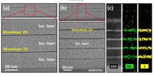
Figure 10. TEM of the deposited 2D/sacrificial material stacks.
Sequential deposition of the 2D materials and sacrificial layers is a far more production type of process versus film transfer and likely to be lower cost as well.
The resulting stacks were then etched into fins using a metal hard mask. Figure 11. illustrates the “fin” formation results.
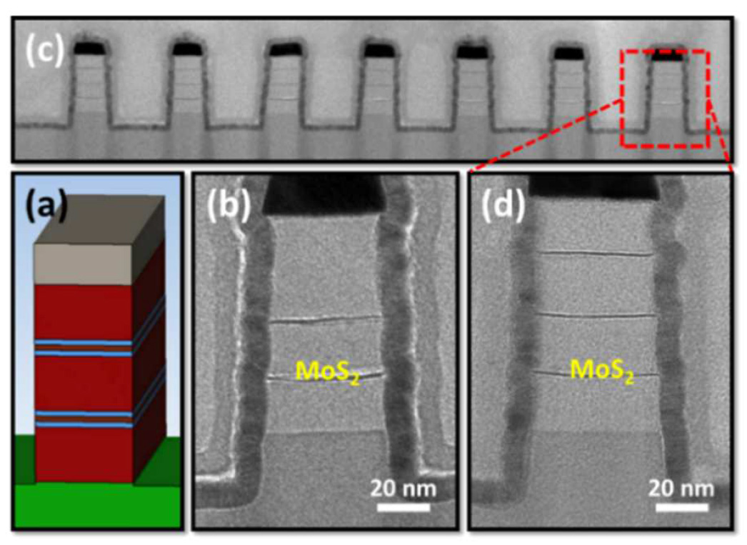
Figure 11. 2D Material stack fins.
As is the case with horizontal nanosheet stacks, an inner spacer is needed to reduce capacitance. To form the inner spacer an additional sacrificial material is needed to prevent collapse of the 2D layers. Figure 12. illustrates the inner spacer process.
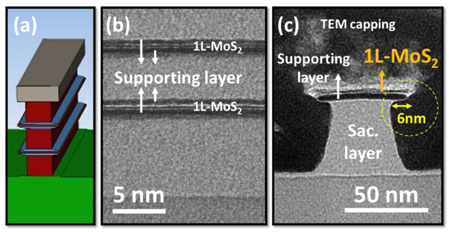
Figure 12. Inner Spacer formation.
Finally, metal edge contacts are formed, and the channels are released. Figure 13. illustrates the metal edge contacts.
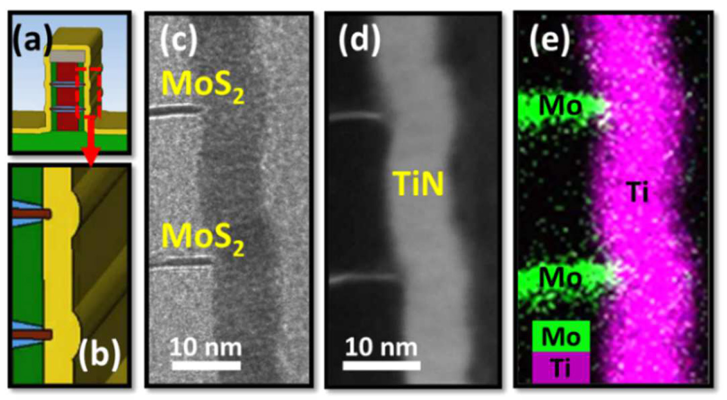
Figure 13. Metal Edge Contacts.
The resulting devices have high contact resistance due to lack of doping in the contacts and extension regions. A 1 layer device with 40nm Lg was demonstrated with a Vth of ~0.8 volts, SS of ~250 mV/dec and drive current of 410 μA/μm.
Conclusion
These 7 papers illustrate both the excellent progress being made toward 2D devices and the level of interest at two of the leading-edge device producers. Some recent projections I have completed suggest that 2D CFETs can achieve logic density 5x of the current densest production standard cells. 2D CFETs are likely a technology for the 2030s as opposed to the 2020s and illustrate that logic scaling is nowhere near being at an end.
Also Read:
IEDM 2022 – Ann Kelleher of Intel – Plenary Talk
Share this post via:


Comments
6 Replies to “IEDM 2023 – 2D Materials – Intel and TSMC”
You must register or log in to view/post comments.