As uncertainties mount about the near-term semiconductor industry from companies in Apple’s supply chain and the significant drop in memory chip prices, the semiconductor industry has consistently grown each year since the great recession of 2009. Semiconductor revenues have consistently outpaced semiconductor equipment revenues, which I discussed in a November 27 SemiWiki article entitled “The Disconnect Between Semiconductor and Semiconductor Equipment Revenues.”
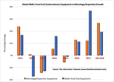
Historically, sales of process control tools have not mirrored sales of the entire front-end equipment market. Chart 1 is a graph of the change in revenues for the year as a comparison between the total equipment market and total process control market. Over the eight years of this chart the cyclicality in capacity-oriented capital spending by logic and memory chip manufacturers is obvious.
In 2017, we witnessed a ramp in memory spending – wafer front end equipment revenues from memory suppliers reached $27.8 billion, up 63.5% from revenues of $17.0 billion in 2016.
In 2012 industry-wide slowdown in memory-related semiconductor capital spending, which decreased 44.7% from 2011 revenues, followed in 2013 by a decrease of 20.9% in equipment spend from logic and foundry companies.

For the first three quarters of 2018, wafer front end equipment revenues increased 19.4% compared to 26.7% for metrology/inspection companies, according to The Information Network’s report “Metrology, Inspection, and Process Control in VLSI Manufacturing.”
A Paradigm Shift in Metrology/Inspection Demand
Semiconductor companies in the past attempted to ensure quality and reliability by using statistical analysis and data analytics capabilities of semiconductor yield-management systems or software. Statistical Process Control for semiconductor manufacturing enables a company to maximize yield and quality by merely sampling a small number of wafers out of thousands processed daily. Thus, the revenue growth in metrology/inspection systems often lags the growth in overall equipment, shown in Chart 1.
However, as semiconductor design rules decrease, yield becomes more sensitive to the size and density of defects. In addition, new manufacturing techniques and device architectures in production, which include 3D finFET transistors; 3D NAND, advanced self-aligned multiple patterning, and EUV lithography are creating a paradigm shift in metrology/inspection demand.
Semiconductor manufacturers decide to purchase metrology/inspection systems based on a number of factors, which when compiled become its “Best of Breed.” These factors include technological innovation, cost of ownership, price product performance, throughput, reliability, quality, and customer support.
Large companies such as KLA-Tencor and Hitachi High Technologies are facing competition from smaller and emerging semiconductor equipment companies, which (1) address specialized markets and (2) utilize innovative technology to gain customers.
For example, Rudolph Technologies’ CEO Michael Plisinski on Q3 2018 noted in his Q3 2018 earnings call his focus on a specialized market:
“Over the years, we’ve steadily grown our position in the RF communications market expanding our customer base to include 4 of the top 5 RF filter manufacturers as well as multiple leading module manufacturers. In fact, this quarter, we sold systems for RF process control to 7 different customers. The majority of these systems were to support investments in the manufacturing of sub-6 gigahertz devices for the initial build-out of 5G infrastructure.”
RF communication devices is currently a $10 billion market (total semiconductor market is $450 billion), but demand will mushroom with the introduction of 5G networks coming in 2019.
As an example of smaller companies utilizing innovative technology, RTEC recently introduced a new product, NovusEdge, for bare wafer edge and backside inspection. Edge die yield is becoming even more critical as semiconductor manufacturing fabs attempt to save costs by reducing the wafer edge exclusion to produce a larger number of yielding die per wafer.
Rudolph estimates the total available market for edge and backside inspection in this market to be roughly 15% to 20% of the overall unpatterned inspection market, which according to The Information Network was $435 million in 2017.
There are several startups gearing to compete against market leader KLAC. FemtoMetrix (Irvine, CA), uses Optical Second Harmonic Generation (SHG), a non-destructive, contactless, optical characterization method to characterize surfaces, interfaces, thin-films, as well as bulk properties of materials. Already, FemtoMetrix has completed its first round of equity financing in a deal led by Samsung’s Venture Division and SK Hynix Ventures, and announced a license agreement with Boeing. This type of new technology will eventually compete against KLA-Tencor.
Metrology/inspection equipment companies will benefit from the growth of the semiconductors in general, and from the need to increase in chip quality and reliability as the industry moves to 3D logic and memory chips, and more advanced technologies such as EUV lithography become more commonplace.
Share this post via:


Comments
There are no comments yet.
You must register or log in to view/post comments.