Smartphone shipments have been dropping over the past few years, as shown in Chart 1, as a result of several factors, but primarily the slowdown in smartphone innovation while at the same time prices have kept increasing. Even with the much anticipated 5G in 2020, unimpressive speed gains coupled with a Covid-19 backdrop, smartphones unit shipments may drop another 4% in 2020.
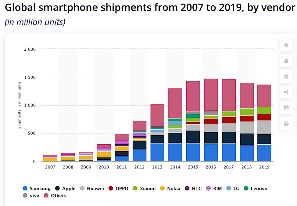 Chart 1
Smartphone manufacturers continue to add features to smartphones, such as multiple cameras or more memory, even though these have not been able to incentivize subscribers to shorten upgrade cycles. One feature that smartphone manufacturers have changed is the type of display, migrating from LCDs to rigid OLED displays to Flexible OLED displays to Foldable OLED displays.
Table 1 illustrates this transition in display type. While global smartphone shipments will exhibit a CAGR (Compound Annual Growth Rate) of -0.4% between 2017 and 2022, LCD display shipments will exhibit a CAGR of -6.7% while OLED displays will exhibit a CAGR of 11.9%.
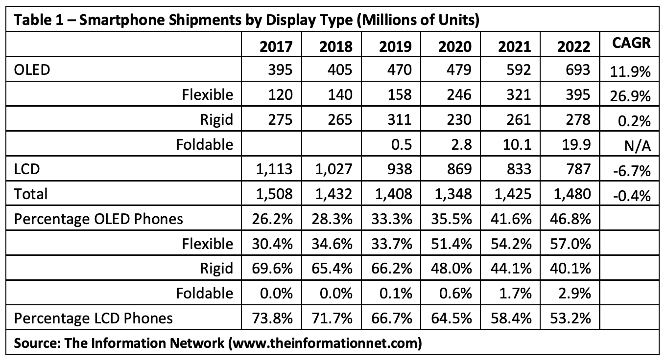
In addition, within the OLED display sector, rigid OLED displays will exhibit a CAGR of 0.2%, while flexible OLED displays will exhibit a CAGR of 26.9%, according to The Information Network’s report entitled “OLED and LCD Markets: Technology, Directions and Market Analysis.”
I expect stronger growth in flexible OLED displays in 2021 coming from Apple (AAPL), which in 2020 its iPhone 12 models all have flexible OLEDs, as sales of these models, which shipped late in 2020 will continue in 2021, along with iPhone 13 models.
Foldable smartphones will grow from just 500,000 units in 2019 to 19.9 million in 2022. A total of 2.8 million foldable smartphones were sold in 2020, as Samsung’s Galaxy Z Flip smartphone Galaxy Z Fold 2 accounted for 73% of them.
Strong Growth in Flexible and Need for Encapsulation
A major problem with OLEDs is that the organic layers in the devices are extremely thin, and most of them are based on chemically active materials, which are easily damaged by exposure to moisture or oxygen in the air.
To prevent rapid device degradation, rigid OLEDs are encapsulated with a glass lid, which provides an acceptable level of WVTR (water vapor transmission rate). The brittle nature of glass, however, limits its application to rigid OLEDs, and the process is illustrated in Chart 2.
 Chart 2
For flexible OLEDs, a glass seal is not suitable, and a thin-film encapsulation (TFE) is required that is flexible yet provides a robust hermetic seal. Chart 3 illustrates the utilization of TFE for a flexible OLED display. Since it uses a thin film instead of glass for encapsulation, the overall thickness of a display panel is also decreased.
 Chart 3
I refer readers to a comprehensive analysis of OLED encapsulation in my May 24, 2016 Seeking Alpha article entitled “Applied Materials Stock Bounced On Display Orders – But Is It Sustainable?”
Since that article was written, the utilization of flexible OLEDs into smartphones has increased from less than 25% to more than 35% (Table 1). As a result, the structure and deposition processes for the TFE are increasingly being scrutinized. Microscopic pinholes or microcracks that may form during deposition of the TFE or when bending the device result in rapid device failure.
The increasing number of foldable smartphones adds another level of complexity in the design of the OLED and TFE due to the extreme strain and stresses placed on the OLED structure. Add to that the plethora of applications such as automotive, tablets, smart home, and TVs, and the number of TFE applications substantially increases.
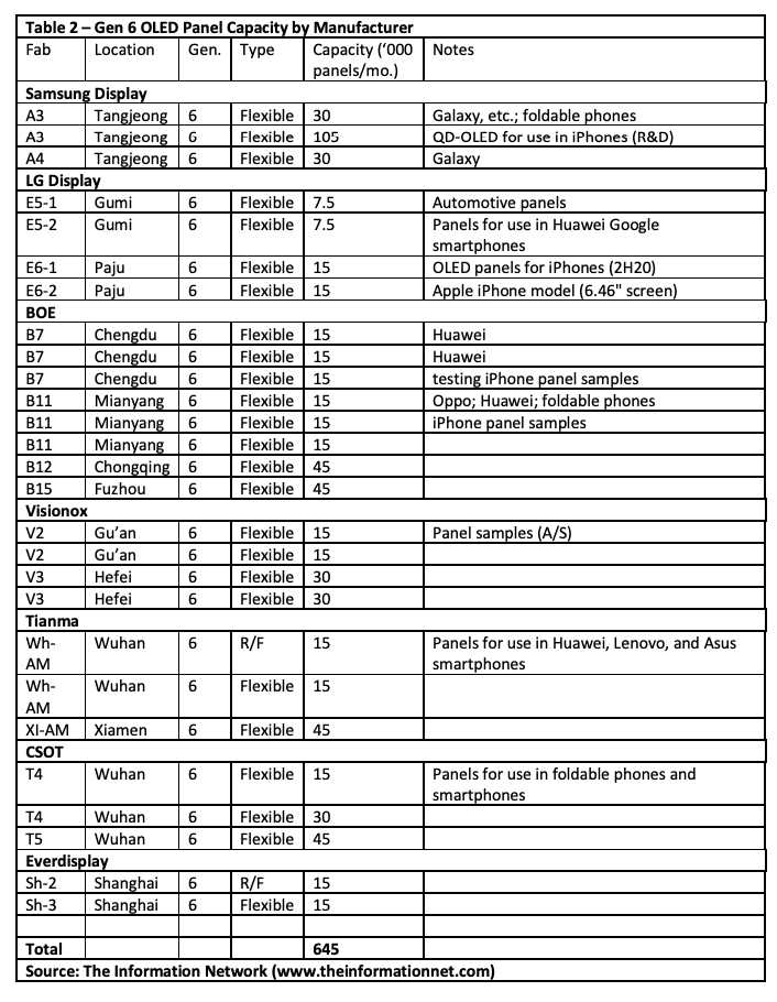
Remember that foldable smartphones are made with modified flexible OLEDs. There are numerous OLED manufacturers with flexible OLED facilities located in Asia with a total capacity of 675,000 Gen 6 panels per month with a motherglass measuring 1500mm ×1850mm, as shown in Table 2.
To put things in perspective,
- 212 iPhone 12 or comparable sized smartphones with a display measuring 146.7 x 71.5 mm can be cut from aGen 6 motherglass panel
- A plant with a capacity of 15,000 motherglass panels per month can produce 38 million iPhone 12 smartphone or comparable sized displays per year.
- The total capacity of 675,000 Gen 6 motherglass panels per month (Table 2) can produce 1.7 billion iPhone 12 or comparable sized smartphones per year.
- 106 foldable smartphones with a display measuring 146.7 x 143 mm can be cut from a Gen 6 motherglass panel
This total capacity of 1.7 billion flexible smartphone displays is 7X the 246 million flexible smartphones made in 2020 (Table 1), in which 212 iPhone 12 display panels can be cut from each motherglass or 106 foldable smartphones can be cut. If a 10-inch tablet is demanded, just 78 panels can be cut.
Problem in Apple’s OLED Supply Chain
Apple has accelerated its innovative drive in its products in the past year or so:
- It moved to OLED displays for all its new model smartphones in 2020 versus top of the line only models in previous years.
- Apple moved from a CISC to an ARM architecture (named M1) as the CPU for its Mac laptops in 2020.
- Apple is looking to release an iPad with a mini-LED display in H1 2021. Now we hear that Cupertino is also planning an OLED iPad Pro release sometime in the second half of 2021 with panels procured from Samsung and LG Display.
- Apple has been known to be working on foldable display technology for some time, filing multiple patents regarding the technology. Samsung is rumored to be providing foldable display samples to Apple for a future foldable iPhone back in September 2020. Samsung is reportedly providing Apple with samples for one year, suggesting that Apple is ramping up work on a foldable iPhone.
But based on my sources, Apple is finding problems with encapsulation technology from Samsung Display (OTC:SSNLF) and BOE Technology, both display suppliers to Apple.
First, Samsung’s TFE processing is undergoing some upheavals:
- Samsung Display has been preparing to separate TFE equipment suppliers in its supply network. Samsung Display is currently only using Applied Materials’ (AMAT) CVD systems for its Gen 6 OLED production lines. However, it had been looking for a change for its Gen 6 QD display. Wonik IPS, which is one of Samsung Display’s key partners, had participated in R&D process of QD Display and had hoped on developing a system that can replace Applied Materials’ systems. Samsung changed its mind and stayed with AMAT.
- My sources in Korea tell me that Samsung is concerned because the takt time (rate at which you need to complete a product to meet customer demand) to put the glass through AMAT PECVD and Korean ALD (atomic layer deposition) is too long.
Second, there are problems at Chinese display supplier BOE Technology. According to a November 19, 2020 article in MacRumors,
- Chinese display maker BOE has reportedly failed yet again to secure a supply order from Apple for OLED panels for iPhones. BOE is still facing manufacturing issues at its Chengdu plant in Sichuan province, meaning the display maker has failed to secure Apple’s validation for the OLED screens for the second time this year.
- BOE’s plant in Mianyang – in the same province – suffered the same fate in June 2020, due to a low production yield rate of around 20 percent.
- BOE failed to pass Apple’s quality tests and did not become a supplier to the iPhone 12 series (BOE also failed to pass Samsung Electronics’s display quality test).
According to a new report from Korea, Apple has tested BOE’s AMOLEDs for next year’s iPhones, but again BOE’s OLED production quality is not good enough for Apple, which means that in 2021 Samsung Display and LG Display will remain the exclusive OLED suppliers to Apple’s phones.
But then we learned in late https://www.gizchina.com/2020/12/24/finally-boe-has-passed-apples-certification-to-supply-iphone-12-oled-this-month/, that recent reports out of China claim that BOE has finally passed Apple’s certification and will start supplying OLED panels to iPhone 12 products in the near future.
Finally, Apple is advertising for job OLED encapsulation technologist positions:
Come work for the Apple’s OLED Encapsulation team comprising of amazing engineers who make the best OLED displays in the world including the Apple Watch and the iPhone. We make the world’s most reliable thin film encapsulation for OLEDs with worlds best electrical, optical and mechanical characteristics while achieving the small display bezels.
In this position, you will play a critical role in pushing the boundaries of OLED encapsulation for next generation of products. To do so, you’ll be working on core-technologies behind Thin Films deposited though Low temperature ALD, PECVD. With this core know how as a springboard, you will be creating next generation OLED displays with unique product design and the best optical and mechanical characteristics. You will be working on these technologies with Apple’s OLED display vendors across the globe to bring them from prototyping to mass production.
Depending on whether BOE is accepted as a supplier for the iPhone 12, the three suppliers are:
- Samsung Display will produce the flexible OLED panels in its A3 fab in South Korea because it is equipped with the Y-OCTA technology.
- LG Display will produce the flexible OLED panels in its E6 fab in South Korea
- BOE will make the iPhone 12’s flexible OLED in its B7 and B11 fabs in China;
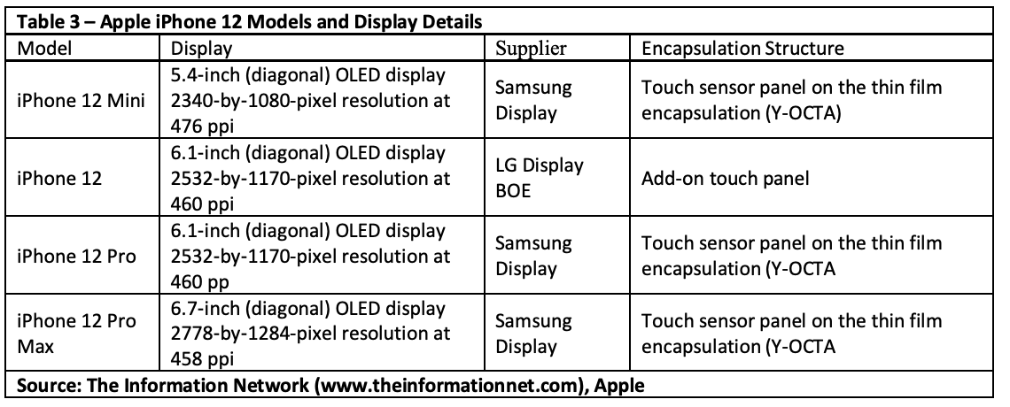
The 5.42-inch and 6.68-inch models are adopting the touch sensor panel on thin-film encapsulation (TSP on TFE), which Samsung Display refers to as Y-OCTA. Samsung Display will supply these two models. However, LG Display and BOE are not yet ready with the TSP-on-TFE technology. Therefore, the 6.06-inch, which LG Display is the main supplier of and possibly BOE, is equipped with the add-on touch panel.
Table 3 shows the four iPhone 12 models, and the display details and supplier.
TFE Process and Equipment
Table 4 shows a comparison between ALD, CVD and PVD deposition techniques

The PVD films exhibit relatively low film quality, with many defects and pinholes in the film, and the PECVD films can cause plasma damage and high process temperature issues. In contrast, ALD enables the thin film to be stably deposited at a low temperature in a vacuum chamber, and to be almost defect-free, but is 1000 times slower than the other processes.
Single-layer TFE has been attractive because it has a simple fabrication process compared to other encapsulation methods. But multilayer technologies address the aforementioned issues by inserting an interlayer. This can improve the WVTR by increasing the lag time. The flexibility can also be improved by the newly inserted layer. The inorganic layers (such as SiNx, SiOx, Al2O3) serve as the main barriers to block the moisture. Since defects such as pinholes and other particles unavoidably occur, organic layers (such as epoxy resin, phenolic resin, PET, PBT) effectively block the moisture infiltration paths.
Applied Materials, as mentioned above, is used for TFE for Samsung’s Gen 6 flexible OLEDs. It’s Enflexor Gen 6H PECVD deposits a range of buffer barrier films. AMAT’s TFE process is proprietary, but we can learn a bit from its patentfiled in July 2018. The encapsulant can include a first barrier layer, a buffer layer, and a second barrier layer.
The first barrier layer can include a dielectric film, such as SiN (silicon nitride). The buffer layer can be an organic layer, such as a hexamethyldisiloxane (HMDSO) layer. A second barrier layer comprising SiN is then deposited over the buffer layer.
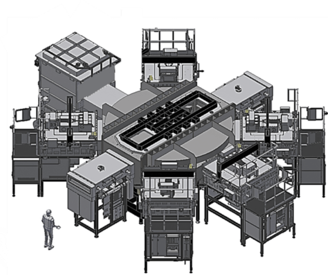
AMAT’s Enflexor Gen 6H system is shown in Chart 4, showing the size and complexity of the cluster tool. This description of multiple layers using multiple process chambers explains the need for such a large and complex AMAT system, and can be explained in further details in the patent:
“A method of encapsulating an organic light emitting diode OLED device, comprising: generating a first plasma comprising silicon and nitrogen in a first process chamber; depositing a first portion of a first barrier layer comprising silicon and nitrogen over the OLED with the first plasma; generating a second plasma comprising silicon and nitrogen in a second process chamber; depositing a second portion of the first barrier layer comprising silicon and nitrogen over the first portion of the first barrier layer with the second plasma, wherein a density of the first plasma and the second plasma differ by a factor of at least 100; depositing a buffer layer over the first barrier layer in a third process chamber; and depositing a second barrier layer over the buffer layer in a fourth process chamber, wherein the first process chamber, the second process chamber, the third process chamber, and the fourth process chamber are arranged around a single transfer chamber.”
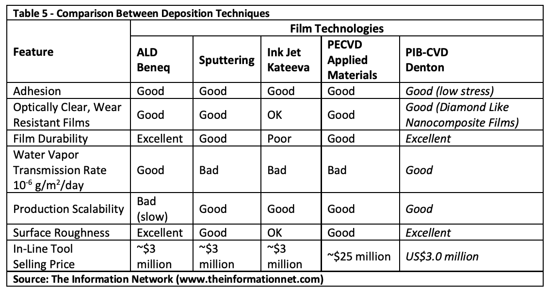
Using a unique technology for the display market, privately held Denton Vacuum (Cherry Hill, NJ) uses ion beam technology to deposit a Diamond-like nanocomposite organic layer sandwiched between two SiOxNy dielectric layers to form the encapsulant. But the equipment is priced at $3 million compared to an estimated $25 million for AMAT’s Enflexor.
To achieve a throughput of 1 Gen 6 motherglass panel per minute, the Phoenix In-Line PIB-CVD Deposition System is configured with 6 chambers with 2 linear sources in each chamber. Three chambers for each of two materials (inorganic and organic), PIB-CVD of Inorganic SiOxNy and Organic a-C:H DLN
- Stress Control: 0 to 10MPa
- Water Vapor Transmission Rate <1E-6 g/m2-day
- Deposition Rate > 2500A/min
- Good Adhesion
- Deposition Temperature < 100C
Table 5 compares the commercially available techniques.
TFE Equipment Market for Flexible and Foldable Smartphones
Applied Materials is the market leader in TFE equipment, primarily because of its established history of deposition equipment in displays, starting with the 1993 formation of AKT (Applied Komatsu Technology) with Japan’s Komatsu, and the acquisition of the remaining 50% from Komatsu in 1999.
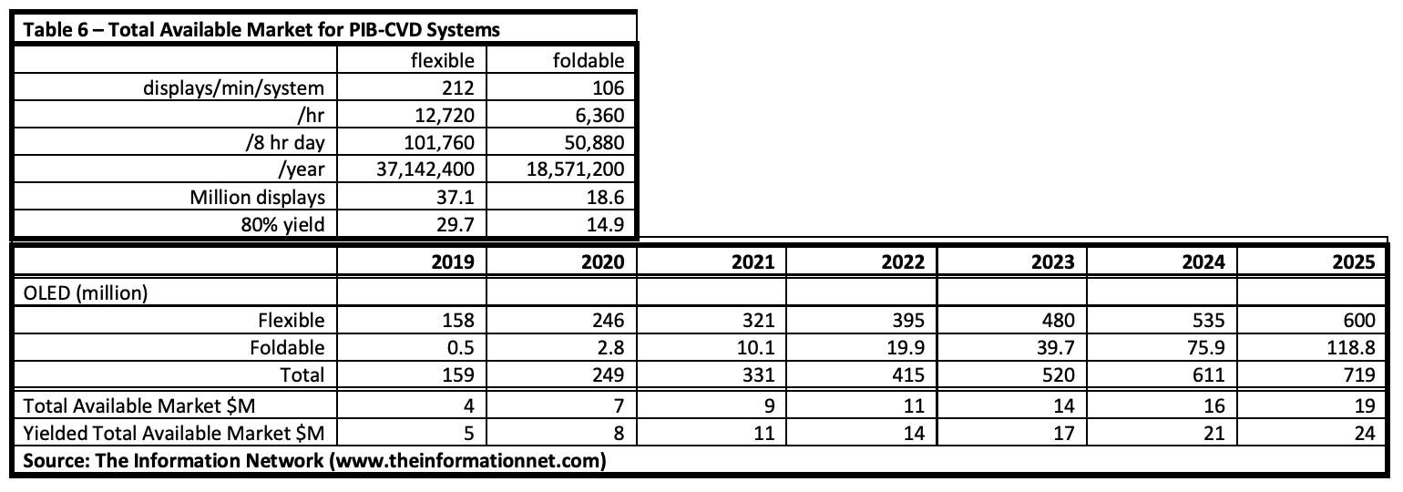
Table 6 presents an analysis of the total available market for competitor Denton Vacuum using its PIB-CVD Systems, which I chose based on price/performance of the systems. My analysis is based on a model for displays using Gen 6 Glass (1500mm x 1850mm), coating 212 6.1” flexible displays/motherboard and 106 foldable displays/motherboard at one time, and a throughput of 1 motherglass per minute for the deposition of the TFE. Based on an 80% yield and the system operating 24 hours per day, 365 days per year, system revenue per year is shown.
But based on my analysis, Apple’s scrutiny of Samsung’s encapsulation, which uses AMAT TFE equipment, and BOE Technology, which also uses AMAT TFE equipment, is a headwind for AMAT from two standpoints:
- High-Priced Equipment, estimated at $25 million
- Better Technology at significantly lower equipment price from competitors
If we compare the Yielded Total Available Market in Table 6 at $5 million and $8 million for Denton’s equipment in 2019 and 2020, AMAT registered, at 8X the selling price of the system) revenues of $40 million in 2019 and $64 million in 2020. Going forward, the revenue growth for Denton’s $3 million system would mean lost AMAT revenue multiplied by eight.
Share this post via:



Comments
4 Replies to “Apple’s Priority On Improved OLED Encapsulation For Foldable Smartphones Will Impact Applied Materials”
You must register or log in to view/post comments.