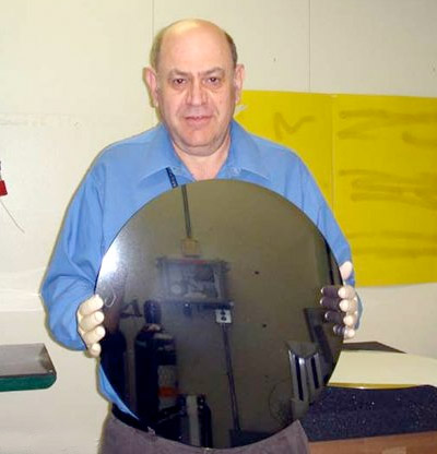
 I’ve been digging around the Interwebs a bit trying to find out what the received wisdom is about how big a cost reduction can be expected if and when we transition to 450mm (18″) wafers from today’s standard of 300mm (12″). And the answers are totally all over the place. They vary from about a 30% cost reduction to a cost increase. That is, 450mm wafers may cost more per square cm than 300mm.
Here are some of the issues:
Creating wafer blanks. It is currently very expensive and not expected to come down to equivalent 300mm costs. It turns out that pulling an 18″ ingot of silicon has to be done really slowly because of various stress reasons. A 450mm wafer blank is expected to be twice the price per area of 300mm.
Double patterning. There is some saving during lithography using 450mm versus 300mm because you don’t have to switch from one wafer to the next so often. But the main litho step of flashing the reticle on each die has no gain from having more die on the wafer. A flash is a flash. And with double patterning that step is a bigger fraction of the whole manufacturing process. Oh, and don’t think EUV will save the day completely. It is so late that the earliest that it can be introduced is maybe 9nm and expectation is that EUV will require double patterning (it is 13.5nm light, although I don’t really understand why the OPC techniques we used to get, say, 90nm with 193nm light without double patterning won’t work, but I’m not an expert on optics).
Since 450mm wafers hold roughly twice as many die as 300mm, any given volume involves half as many wafers so, except for the highest volume parts like flash, there will be an increase in the number of machine setups (fewer machines, fewer fabs, but more switches from lot to lot).
Cost of equipment. This is the biggie. If 450mm equipment only costs about 1.3X 300mm equipment then the future is probably rosy. But there are people out there predicting cost increases of 3X which will make the transition economically infeasible.
Capital efficiency. The big advantage, if 450nm is a success, is that it is more capital efficient. It doesn’t take so much capital to get the same capacity in place. But if that is really so, can the semiconductor equipment industry survive?
Process generations. Received wisdom is that only around now are semiconductor equipment manufacturers through their R&D costs and starting to make money on their investment for the 300mm transition. That’s a lot of process nodes. How many more nodes will there be (with current equipment) to recover any 450nm transition?
Who wants it? Intel and Samsung. TSMC is apparently a reluctant guest to the party since their business requires smaller runs and lots of changes from one design to another, so realistically their cost savings will be less than Intel and Samsung whatever happens.
Human resources. Developing new processes to keep on the 20nm-14nm-9nm transition already is arguably short of people since it has become so demanding. Where are the people going to come from to manage the 450nm transition? If we get 450mm but not 14nm what does that do to costs?
SEMI, the semiconductor equipment association, has been against 450nm. Almost everything they have written for the last 5 years has been against it. I can’t see how it will be a win for them. In fact, I think the Intel/TSMC/Samsung investments in ASML are an acknowledgement of that. The R&D investment has to come from the end users of the equipment.
Here’s a SEMI quote, admittedly from 2010:”450-mm wafer scale-up represents a low-return, high-risk investment opportunity for the entire semiconductor ecosystem; 450-mm should, therefore, be an extremely low priority area for industry investment,” says a recent SEMI report.
OK, so that’s not very informative and I haven’t come across anything that convinces me that anyone really knows the answer. But there is a lot of food for thought.


Comments
14 Replies to “How Much Cost Reduction Will 450mm Wafers Provide”
You must register or log in to view/post comments.